The Murgen Project
The hardware design process is fraught with pitfalls, from library component sketchiness, parts availability, erroneous data sheets, underestimates of complexity and long lead times. Designing good hardware on time, on budget and to specifications is like being in a knife fight. Hardware will cut you.
What is this project?
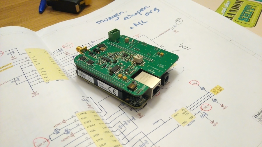
Today, we have achieved the electronic design of the kit and are having it made by a PCB Assembly – someone to actually assemble the probe, and we're waiting for a first prod so that we can physically test it with our in house transducer.
That’s cool! And if you want to learn more (apart from this Readme), you can surf the internet and :
- Read the the Hackday Blog of the fork !
Results ?
Setup
The working place
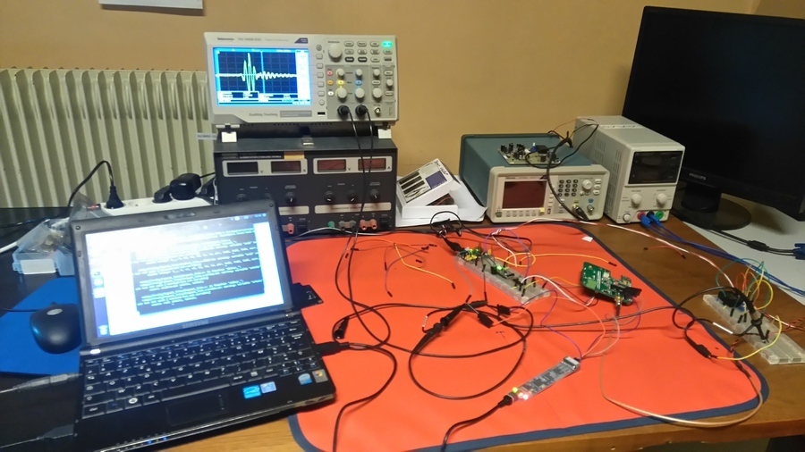
Images
A first picture of our baby !
Disclaimers
Disclaimer: though an engineer, this project is the first of its sort, we never did something related. Bear with us, and the discovery process – we’re happy to learn on the way =)
Disclaimer #2: ultrasound raises questions. In case you build a scanner, use caution and good sense!
Teaser
Folders
hardware/            main repo
|-- Altium            the altium files for Murgen -- source files, opening with Altium Designer
|-- BOM                that's ... well.. for the BOM
|-- Gerbers            to build the cape
|-- 3D                for the 3D files of the board
|-- tobo            simplified pulser
`-- goblin            an alternative, in Eagle
You will also find the CHANGES.TXT, CONTRIB.TXT and LICENSE.TXT at the root.
Schematics are in the Altium\Schematics\PDF folder
Project introduction
Brief
Disclaimer: this brief does not rock. It is crappy, but, well, we live to learn.
In October 2015, we were working on a open-source ultrasound imaging device, and had started to get some result. However, we were facing a bottleneck that is data acquisition and transfer.
Roughly, the aim of the device is to excite a 3.5MHz piezo through a 100V or more, 0.2µs, signal to acquire a signal coming from the echoes.
Once it comes back from the transducer, one needs to cap it, amplify it, filter it, apply a time variable gain to the signal, have it get through a high speed ADC (40MHz at least), and serve it to the the processing unit (through PINs, SPI, USB ?), possibly with a CPLD/FPGA (or DSP / microcontroler ?) in between.
As the data we have should have at least 16 imgs / sec, with 64 lines, the rate shall be around 120Mb/s, and to avoid the data transfer bottleneck (see Estimating datarates), we were thinking of leverage the capacities of raspberry (or beaglebone) and such to have shields/capes that can be used and connect through SPI for example to the raspberry where raw data can be processed, and image can be going out, hence a lower rate.
A bit more context
The board
The board in itself is not a medical device. The board is a dev kit for the analog part that one could find in any ultrasound probe. It respects the functions and blocks one can find in basically any probe (pulser, TGC, ADC, ..). A main difference is that this board is designed for a single element, and provides so far only a minimal support for the mechanics behind image formation.
Having a single element allows for more space, less density, and to go straight to a regular, though relatively high-speed ADC.
The Process
None of us had already done an electronic product, so the process in not that of an experienced team, and we're learning on all the fields: writing down an idea, analysing it, structuring it, develop the plans, build it, test it, build the software.. Rince and repeat.
The most challenging part, and somewhere the easiest, will be to allow anyone with little or no experience to replicate our efforts, and to build another copy of the board. Why is that so? With fresh eyes, that's easier to understand what the blocking points could be, what needs to be detailed, and how.
Debug Sessions
Finding the short
The notes are here (the murgen-1.0-short-issue.md file). We found the bug, two main issues are to be corrected on board v1.1:
- A short on the ADL5511
- The RECOM has to be mounted upside down, as the pin layout were inverted during the design stage
Playing with the board
The notes are here, stemming from the work sessions with the board:
- Session 1 : Powering the board, power use, first (bad) trigging and echoes (06 March 2016)
- Session 2 : Non-controlled pulsing, inverters, better echoes (11 March 2016)
- Session 3 : Getting controlled pulsing, but width not controlled (15 March 2016)
- Session 4 : Width of the pulses is getting controlled =) (19 March 2016)
- Session 4b : Simple data visualisation with BitScope (19 March 2016)
- Session 5 : moving the transducer to get the first image (20 March 2016)
- Session 6 : Getting a clinically usable image (28 March 2016)
- Session 7 : Getting cleaner images - code improvements (3 April 2016)
- Session 8 : Comparing acquisition speeds (3 May 2016)
- Session 9 : Playing with ATL10PV (3 July 2016)
- A more complete hardware ReadMe : Information, and more, with a focus on the electronic part of the project
- A more complete software ReadMe : Information, and more, with a focus on the code part of the project (arduino, python, and such)
Preliminary questions
Why are we making this?
Because it’s fun, it the first step towards medical open hardware based on ultrasounds, so it’s an element for echOpen ! And because existing hardware doesn’t come in for low-cost, rough uses.
Who is this for?
This element, comprised of the analog part of ultrasound imaging processing, is aiming hackers, makers, … all who can have fun prototyping a low-cost ultrasound device.
How will this be used?
This shall be used in conjunction with the mechanical unit (motor, encoder, transducer), and plugged into a small processing unit (aka Raspberry, or BeagleBOne Black for exemple)
What features does it need to have (now)?
Be able to emit a ultrasound pulse at high voltage, and receive a signal, clean it, detect the envelop and ADC it.
What features does it need to have (later)?
Shifting envelope detection to software once we’re sure the processing works at “low” rates.
What are the legacy requirements?
Nothing yet, except a couple of constraints on the use of the tool.
Who’s going to build this?
Makers, doers, academics, … can use this. But we’d be happy to go with a PCB assembler at first!
How many do we want to make?
At first, a couple, to prototype it. Once prototyped, this board could be in the hundreds.
What is the timeline?
The objective is to get a first functional prototype by February 2015.
What are the Goblin and Tobo stuff ?
Those are two alternatives to murgen, in the sense that components may not be the same for goblin, and that tobo is a mini-murgen, limited to the pulser. Goblin is a simpler version, a two-layer one, but we'll need funds to test this one out =)
Requirements to build the board
BOM
In the BOM folder !
At the fab
PCB
A 4-layer PCB.. not so cheap, but at the same time..
Fab
Lots around... choose what you want =)
Links
PCB Maker:
- seeedstudio.com
- PCBshopper.com
PCBA abroad :
- myropcb
- nortechsys
- SeeedStudio only north america
PCBA in france:
- Quad Ind
- PCB-Pool
- EdgeFlex
Costs
With the french fab we're working with, costs sum to 160e, and they are split as follows, prices being without taxes:
- PCB : 7.34e (but there are overcosts to produce the masks, ...)
- Components : 143.5e and T1-6T-KK81+ (sold by 10): 9.34 each, but can come down to 140e with some volume.
In this case, assembly is close to 120e.
Technically
Principles of echography
Basically, echography means plotting echoes. It means we have to create a sound pulse (2), use a good sensor (2), find a way to transform a 1D signal to a 2D image (3), listen to the echoes coming back, cleaning them and processing them to create an image the way a bat would do (4), and to transmit them to a display (5). 5 steps.
The present project aims at taking care of (1), (4) and (5) - meaning amm electronics related to the analogic part of the imaging.
Narrative of the flow
Since we're using a single sensor (not an array of sensor, as those are used in "regular" machines), we don't have the Beamforming parts. The sensor is similar to a speaker, in the sense that it can be used to generate an acoustic signal from electricity, and vice versa. The flow is therefore as follows:
- A pulse generator generates a high negative voltage pulse, which is as low as possible and to excite the transducer (or crystal), which will resonate at his central frequency. In our case, this is 3.5MHz, but that depends on the transducer being used.
- A signal will come back through the echoes, the reverberation of the acoustic waves on "obstacles", exciting the transducer, having it generate an electric signal.
- This will be prepared by a switch. Indeed, the signal needs to be separated from the excitation. Excitation being at -150V, the signal coming back will be in mV - and it needs to be isolated.
- The signal usually goes through a LNA - low noise amplifier - to be amplified
- then it's processed by a TGC to compensate for signal attenuation. Indeed, the deeper the echoes come back from, the more attenuated they are, and this needs to be corrected.
- An AAF (Anti-Alias Filte) can be put in between, and in the case of the first Murgen release, we also include an enveloppe detection: indeed, echoes are signals that are coming from a couple of ultrasound periods reflected on interfaces, and what interests us is not (at first) the signal itself, rather the enveloppe of it.
- The "cleaned" signal goes through an ADC to be digitalized
- this is output to buffers, in our case to protect the BBB GPIOs.
Data rates and key figures
- We're aiming at 128 lines/image - that may be enough at first
- at 16 imgs/s, that's 2048 lines/s
- That's 488us per line (for everything:
- Let's image no further than 15.77cm deep.. Why? Because : -(15.77 cm x 2) / (154000 cm/s) = 204.805 us -that's 1024 pts at 5MHz -That's 204.805 us per line -That's 283.5 us of idle time - kept for processing, and whatnots
- Final image is therefore 128*1024 px -1024 pts for 15.77cm is 6.49px / mm -That's also 2.1Msps on average or 24Mbit/s.. borderline for data transfer on certain systems.
Discussions
The bottleneck may lie in the data transfers...
Data rates and Data bus
- 151202: QuadSPI through a dedicated microcontroleur?
- 151201: At 5Msps, 12 bits, shall we use SPI or parallel?
- 151201: SPI is managed through hardware... parallel, not. Has to be managed from soft. Can be an issue for real time, and to avoid loosing samples.
- 151130: Rather be going onto SPI : QuadSPI? Is that managed by the RPi? Common amongst ADCs ?
- 151207: For high speed data acquisition: about 120Mbits/sec: No SPI port will support such speed…. Only the Quad version… we can use USB 2.0 HS for such huge movement. A FPGA or FPGA/RISC MPU combination can be the best solution. Later, once on RPI, the data can be handled. But for so perfect measurement of times, and value, only a DSP it’s not enough.
Signal detection
- 151129: LTC5507ES6 to filter ? A rajouter!
ADC and DAC
- 151130: Better ADC at LTC2315-12
- AD7356 (ual, 12-bit, high speed, low power, successive approximation ADC that operates from a single 2.5 V power supply and features throughput rates up to 5 MSPS.
- DAC: a simple DAC i2c
Different setups
- 151202: A DSP may be sufficient for our needs: is that the case?
- 151203: Proposed setup
- Using a a Main controller - STM32F407 + USB High speed PHY ??
- Analog frontend : 1/4 of AD8264 as LNA and VGA + AD9236 ADC. TGC can be controlled by internal STM32 DAC - that's max 100-point TGC calibration curve. The ADC then could be connected to DCMI interface of STM32.
- Transmitter: could be HV Pulser and the TR switch - microchip HV7360 + MD0100, STHV 748
- 151209: In looking at the issue, I think that DSP can be implemented. Of course, that comes with the sourcing and a bit of programming, but it should work and provide some flexibility.
- 151112:
- it'd be interesting to keep a 100M s/s sampling rate.
- wouldn't recommend MD1210 and TC2320 from supertex for the pulse part. Those have a recovery time that is quite long, and can get easily damaged - not to mention that they may be obsolete.
- Wouldn't recommend two VGAs ... difficult to control, with a high risk of saturation.
- it'd be interesting to keep a 100M s/s sampling rate.
151201 : Electronics for all in one chips: AFE (Analog front end)
Rationale
It appears that compoonent MAX2082 from Maxim's could be a great choice because it integrates everything in one chip (Analog Front End, Pulser, TCG (ou AVG pour eux), T/R Switch, ADC, Filtrage) - maybe better exists ? Note : Pre-existing chips are 8-channels.
Resources
- MAX2082 - Maxim (Pulser +/- 105 V), TCG (ou VGA) , ADC 50 MSPS and filtering (63$ a piece starting at 1000 units) https://www.maximintegrated.com/en/products/analog/data-converters/analog-front-end-ics/MAX2082.html
- Several Maxim's Analog Front end : https://para.maximintegrated.com/en/results.mvp?fam=us_afe
- Pulser - 90 V (16$ a piece starting at 1000 units) : http://www.st.com/web/en/news/n3553d
- A Texas Instrument Dev Kit : http://www.ti.com/tool/tx-sdk-v1
- Several other Ultrasound Analog Front end (all are 8 channels):
- http://www.analog.com/media/en/news-marketing-collateral/product-highlight/AD927x-AD967x-Octal-Ultrasound-AFE-Product-Family.pdf
- http://www.analog.com/en/products/landing-pages/001/integrated-afe-contains-8-ultrasound-rcv-channels.html
- http://www.analog.com/en/products/analog-to-digital-converters/ad-converters/ad9675.html
- http://www.digikey.com/web%20export/supplier%20content/TI_296/mkt/health/afe5809.pdf?redirected=1
- http://www.ti.com/product/afe5801
- Ultrasound Receiver module (32 channel) (maybe not so cheap) : http://www.cephasonics.com/product/ultrasound-receiver-modules-csm913233
Need of a FPGA ?
According to articles and reading, it seems like it will be delicate to proceed without a FPGA for data processing. All "Reference Design" sheets I've read do have a FPGA, or a DSP.... because signals to be processeed are IMHO too fast for a µC.
Microcontroler
- Microchip - a µC PIC24FJ128GC010 - ADC, 12 bit, 10 MSPS : http://www.microchip.com/wwwproducts/Devices.aspx?product=PIC24FJ128GC010
- and its dev board at 100$: http://www.microchip.com/Developmenttools/ProductDetails.aspx?PartNO=DM240015
- ST ant its ADC 12 bit 5 MSPS µC STM32F334R8: http://www.st.com/web/en/catalog/mmc/FM141/SC1169/SS1576/LN1531/PF258875#
- with its dev board at 10 € : http://fr.farnell.com/stmicroelectronics/nucleo-f334r8/carte-dev-32-bits-stm32f334r8/dp/2424210
- Analog Device has a reference list µC : http://www.analog.com/en/products/processors-dsp/analog-microcontrollers/8052-core-products.html
- At analog device, the best seems to be ADSP-CM40XF with a 16 bit ADC at 2,3 MSPS: http://www.analog.com/en/products/processors-dsp/cm4xx-mixed-signal-control-processors/adsp-cm403f.html#product-overview and its 2 dev boards:
- I also found some MCU with an internal ADC and a good rate wich seems interesting : http://www.analog.com/en/products/processors-dsp/analog-microcontrollers/8052-core-products.html and http://www.microchip.com/Developmenttools/ProductDetails.aspx?PartNO=DM240015
Forks
Constraints
- 151124: The tech milestone was on Nov 24th '15 - and we need to have something by mid Feb' 16.
YDO ideas
- 151125: I'm pretty sure that it's impossible that a microcontroler, raspberry or beaglebone can process this data at a speed above 5Msps. Most of ADCs have a SPI interface, with a 12-bit ADC at 5Msps we'd need a SPI at more than 60Mbps - not everything can do ! In such a case, a DSP or a FPGA is a must-have.
LJO/FKA cape
- 151124: let's play with the BBB PRU's and develop a analog+ADC cape.
HV Supply
HV-supply is going to introduce noise in the circuit.. therefore, a home-made booster was not selected, especially when going at 100V+. We had to options to consider:
- Using a MAX1711 in Jatin Sharma thesis, he goes from 12V to 180V. Gerbers and schematics are included in his master). The board was separated from the rest of the design, to avoid any pickup/noise.
- We have tried the R05-100B - a tad more simple, and based on 5V, so easier for us (5V -> 120V). Schematics are simple, introducing only a couple of capacities.
Electronics
So far, the key issue is a compromise in terms of data output. It's interesting to see how to interface such data rates to a processing and display unit.
Setup
Jumper 1
This one represents the fixed Gain for the TGC. An extra 18 dB is always handy!
Jumper 2
todo
ADC Clock:
The 4 options switch allows for a sampling frequency range of choices:
| R1 | R2 | R3 | R4 | Rset Value | Clock Frequency |
|---|---|---|---|---|---|
| 1 | 2 | 3 | 4 | Ohm | [MHz] |
| OFF | OFF | OFF | OFF | Invalid | Invalid |
| OFF | OFF | OFF | ON | 100000,0 | 1,0 |
| OFF | OFF | ON | OFF | 40200,0 | 2,5 |
| OFF | OFF | ON | ON | 28673,3 | 3,5 |
| OFF | ON | OFF | OFF | 27400,0 | 3,6 |
| OFF | ON | OFF | ON | 21507,1 | 4,6 |
| OFF | ON | ON | OFF | 16294,1 | 6,1 |
| OFF | ON | ON | ON | 14011,1 | 7,1 |
| ON | OFF | OFF | OFF | 20000,0 | 5,0 |
| ON | OFF | OFF | ON | 16666,7 | 6,0 |
| ON | OFF | ON | OFF | 13355,5 | 7,5 |
| ON | OFF | ON | ON | 11781,9 | 8,5 |
| ON | ON | OFF | OFF | 11561,2 | 8,6 |
| ON | ON | OFF | ON | 10363,1 | 9,6 |
| ON | ON | ON | OFF | 8978,9 | 11,1 |
| ON | ON | ON | ON | 8239,1 | 12,1 |
Parts, ICs selection (and critical specs)
HV7360: High Speed, ±100V 2.5A, Two or Three Level Ultrasound Pulser
- High density integration AC coupled pulser
- 0 to ±100V output voltage
- ±2.5A source and sink minimum pulse current
- Up to 35MHz operating frequency
- 2.0ns matched delay times
- 2.5, 3.3 or 5.0V CMOS logic interface
- Low power consumption and very simple to use
HV7360 is a high voltage, high-speed, pulse generator with built-in, fast return to zero damping FETs. This high voltage and high-speed integrated circuit is designed for portable medical ultrasound image devices, but can also can be used for NDT and test equipment applications.
The HV7360 consists of a controller logic interface circuit, level translators, AC coupled MOSFET gate drivers and high voltage and high current P-channel and N-channel MOSFETs as the output stage. The peak output currents of each channel are guaranteed to be over ±2.5A with up to ±100V of pulse swing. The AC coupling topology for the gate drivers not only saves two floating voltage supplies, it also makes the PCB layout easier.
Protection: MD0100 Datasheet - HV Protection T/R Switch
- Up to ±100V input voltage protection
- Low on resistance - 15O typical
- Fast switching speed
- Effectively, a simple two terminal device
- No external supplies needed
MD0100 is a high voltage, two terminal, bi-directional, current-limiting protection device. The two terminals are interchangeable. It is designed to protect a low noise receiver from the high voltage transmit pulses in ultrasound applications and is commonly referred to as a T/R (transmit and receive) switch. The MD0100 can be considered as a normally closed switch with a typical switching resistance of 15O that allows small signals to pass.
Once the voltage drop across the two terminals exceeds a nominal value of ±2.0V, the device will start to turn off. In the off state, the MD0100 can withstand up to ±100V across its terminals.
A small amount of current, typical of 200µA, is allowed to flow through.
TGC : AD8331 (Single VGA with Ultralow Noise Preamplifier and Programmable RIN)
- Ultralow noise preamplifier
- 3 dB bandwidth: 120 MHz
- Low power: 125 mW/channel
- Wide gain range with programmable postamp (-4.5 dB to +43.5 dB in LO gain mode, 7.5 dB to 55.5 dB in HI gain mode) – we can use this with the corresponding on-board jumper
- Low output-referred noise: 48 nV/vHz typical
- Active input impedance matching
- Optimized for 10-bit/12-bit ADCs : perfect for us
- Selectable output clamping level
- Single 5 V supply operation : ideal for a 5V board supply!
The AD8331 is a single channel, ultralow noise, linear-in-dB, variable gain amplifier (VGA). Optimized for ultrasound systems, it is usable as a low noise variable gain element at frequencies up to 120 MHz.
Included is an ultralow noise preamplifier (LNA), an X-AMP® VGA with 48 dB of gain range, and a selectable gain postamplifier with adjustable output limiting. The LNA gain is 19 dB with a single-ended input and differential outputs. Using a single resistor, the LNA input impedance can be adjusted to match a signal source without compromising noise performance.
The 48 dB gain range of the VGA makes these devices suitable for a variety of applications. Excellent bandwidth uniformity is maintained across the entire range. The gain control interface provides precise linear-in-dB scaling of 50 dB/V for control voltages between 40 mV and 1 V. Factory trim ensures excellent part-to-part and channel-to-channel gain matching. Differential signal paths result in superb second- and third-order distortion performance and low crosstalk.
TGC Control : SPI DAC : MAX5383
Controls the TGC
- 8-Bit Resolution in a Miniature 6-Pin SOT23 Package
- Less than 1µA Shutdown Mode
- Low-Glitch Power-On Reset to Zero DAC Output
- 3-Wire SPI/QSPI/MICROWIRE-Compatible Interface : perfect for a SPI interface
- Low 230µA (max) Supply Current
The MAX5383 low-cost, 8-bit digital-to-analog converters (DACs) in miniature 6-pin SOT23 packages have a simple 3-wire, SPI™/QSPI™/MICROWIRE™-compatible serial interface that operates up to 10MHz. The MAX5383 has an internal +2V reference and operates from a +2.7V to +3.6V supply.
The MAX5383 require an extremely low supply current of only 150µA (typ) and provide a buffered voltage output. These devices power up at zero code and remain there until a new code is written to the DAC registers. This provides additional safety for applications that drive valves or other transducers that need to be off on power-up. The MAX5383 include a 1µA, low-power shutdown mode that features software-selectable output loads of 1kO, 100kO, or 1MO to ground.
Analog envelop detection: ADL5511 - DC to 6 GHz ENVELOPE AND TruPwr™ RMS Detector
- Envelope tracking RF detector with output proportional to input voltage
- No balun or external tuning required
- Input power dynamic range of 47 dB
- Input frequency range from dc to 6 GHz
- 130 MHz envelope bandwidth
- Envelope delay: 2 ns
- Single-supply operation: 4.75 V to 5.25 V
The ADL5511 is an RF envelope and TruPwr™ rms detector. The envelope output voltage is presented as a voltage that is proportional to the envelope of the input signal. The rms output voltage is independent of the peak-to-average ratio of the input signal. The rms output is a linear-in-V/V voltage with a conversion gain of 1.9 V/V rms at 900 MHz. The envelope output has a conversion gain of 1.46 V/V at 900 MHz and is referenced to an internal 1.1 V reference voltage, which is available on the EREF pin. The ADL5511 can operate from dc to 6 GHz on signals with envelope bandwidths up to 130 MHz.
ADC : AD9220 - Complete 12-Bit, 10.0 MSPS Monolithic A/D Converter
- Monolithic 12-Bit A/D Converter Product Family
- Flexible Sampling Rates: 1.5 MSPS, 3.0 MSPS, and 10 MSPS
- Single +5 V Supply
- Out-of-Range Indicator
- 28-SOIC and 28-SSOP
The AD9221/AD9223/AD9220 combine a low cost, high speed single-CMOS process and a novel architecture to achieve the resolution and speed of existing hybrid and monolithic implementations at a fraction of the power consumption and cost. Each device is a complete, monolithic ADC with an on-chip, high performance, low noise sample-and-hold amplifier and programmable voltage reference. An external reference can also be chosen to suit the dc accuracy and temperature drift requirements of the application. The devices use a multistage differential pipelined architecture with digital output error correction logic to provide 12-bit accuracy at the specified data rates and to guarantee no missing codes over the full operating temperature range.
The input of the AD9221/AD9223/AD9220 is highly flexible, allowing for easy interfacing to imaging, communications, medical, and data-acquisition systems. A truly differential input structure allows for both single-ended and differential input sample-interfaces of varying input spans. The sample-and-hold (SHA) amplifier is equally suited for both multiplexed systems that switch full-scale voltage levels in successive channels as well as sampling single-channel inputs at frequencies up to and beyond the Nyquist rate. Also, the AD9221/AD9223/AD9220 is well suited for communication systems employing IF Down Conversion since the SHA in the differential input mode can achieve excellent dynamic performance far beyond its specified Nyquist frequency2.
A single clock input is used to control all internal conversion The digital output data is presented in straight binary format. An out-of-range (OTR) signal indicates an flow condition which can be used with the most significant bit to determine low or high overflow.
Buffers: 74AC541MTC
- Signal isolation is of high value for measurements at this precision (12bit)
The 74AC541 and 74ACT541 are octal buffer/line drivers designed to be employed as memory and address drivers, clock drivers and bus oriented transmitter/ receivers.
Using the Murgen board
Software / Firmware Summary
Up to v1.0, we're still playing with the board, so there's not interface with the BBB.
However, there's a series of tools to play with the board, one of which being the bitscope, a bit more handy than the redpitaya, and though it is less precise, we do have less issues (trigging, memory, ...) with it.
Typical Application
Playing with a broken transducer in a haribo sweet box to see if you can hack ultrasounds.
User’s Quick-Start Guide
- Install
- BitScope BitLib
- python math tools
- something to code arduino
- Clone this repo
You're good to go !
Others
Goodies
Check out oldTobo -- an stand-alone pulser/receiver board and oldGoblin for an alternative version.
People !
Acknowledgement
- Thanks to echOpen =)
- Thanks to Jerome, Farad, Vincent obviously
- Murgen, Sofian, Amit, Emmanuel, Florent, Bertrand & PHH, Mike in a way, list goes on !
License
Licensed under TAPR Open Hardware License (www.tapr.org/OHL)
Copyright Kelu124 ([email protected] ) 2015-2016
Bibliography
FPGA-related bibliography
- Structuring a whole ultrasound system on a board: an excellent thesis from P. Levesques (Kyvox), File:2011 PhilippeLevesque.pdf.
- A first corresponding article: File:Real-Time Hand-Held Ultrasound Medical-Imaging Device Based on a New Digital Quadrature Demodulation Processor.pdf
- the second corresponding article: File:Novel Low-Power Ultrasound Digital Preprocessing Architecture for Wireless Display.pdf
- Hardware-Software Partitioning of Digital Signal Processing in Ultrasound Medical Devices a Case Study : File:Hardware-Software Partitioning of US probes.pdf
- File:A Single FPGA-Based Portable Ultrasound Imaging System for Point-of-Care Applications.pdf
- File:Low-Cost, High-Speed Back-End Processing System for High-Frequency Ultrasound B-Mode Imaging.pdf
- Extremely interesting too, iPHONE ULTRASOUND By Jonathan Adam, Adam Keen, Dean Santarinala and File:project2_presentation.pdf their presentation
Key general articles (base of inspiration for our dear Emile)
- A single monoelement, low-cost ophtalmic probe using a piezo motor : File:Carotenuto ophtalmic prob.pdf : an excellent article.
- A single monoelement, low-cost USB probe using a CPLD + microcontroller File:Richard low cost probe.pdf, including a great diagram block of the USB probe
- Saijo USB work : Development of an ultra-portable echo device connected to USB port : Resource: File:2004 Development of an ultra-portable echo device connected to USB port.pdf
- A Software-Based Ultrasound System for Medical Diagnosis by Samir Ram Thadani File:1997 These MIT Thadani.pdf : an excellent introduction the overall design of a US probe design dating back from 1997.
- Data processing and transfer in echography : File:Design of an Open-Architecture Ultrasound Acquisition System for Real-Time Processing and Control.pdf
- Transducer parameters: File:A focussed transducer-scatterer model for ultrasonic reference st.pdf
Other
- Projet étudiant, réalisation d'un échographe de poche pour Iphone (très intéressant et très instructif...) : https://courses.engr.illinois.edu/ece445/getfile.asp?id=5167
- White paper de Xilinx : portable ultrasound system : http://www.xilinx.com/support/documentation/white_papers/wp378-Xilinx-in-Portable-Ultrasound.pdf
- Quelques Notes d'applications intéressantes de chez Maxim's : https://www.maximintegrated.com/en/app-notes/index.mvp/id/5765 https://www.maximintegrated.com/en/app-notes/index.mvp/id/5553
- Note d'application de chez ST sur "Ultrasound Imaging" :
- Pulser TI avec Applcation Note d'une solution complète avec des composants TI :