Building a Raspberry Pi based ultrasound imaging development platform
Introduction
This project has a specific target of providing a low-cost, open source technological kit to allow scientists, academics, hackers, makers or OSHW fans to hack their way to ultrasound imaging - below 500$ - at home, with no specific equipment required.
Objective
The aim of this project is to build a small ultrasound imaging hardware and software development kit, with the specific goal of:
- building an analog "debugging tool" to explore ultrasound imaging systems.
- consolidating existing hardware research;
- simplifing / lowering the cost of the kit;
- providing a benchmark of ultrasound systems;
- introducing a simple API to control hardware;
- having a server which provides raw ultrasound data, and for ultrasound imaging, can deliver standard DICOM files;
- having a kit that can be used for pedagogical and academic purposes - not to mention people who want to understand ultrasound!
Previous project has shown the feasibility of the hardware, but was not simple enough. Let's keep the momentum, and use this dev kit in other projects as well - such as dopplers or non-destructive testing, different projects using piezos as sensors.
Architecture
Ultrasound imaging has evolved since the first ultrasound machine appeared. The first devices were using single-sensor (transducers) techniques, coupled with mechanical scanning - hence allowing a single signal processing channel. The architecture of such systems, as shown below, is well-known and formed the basis of ultrasound imaging.

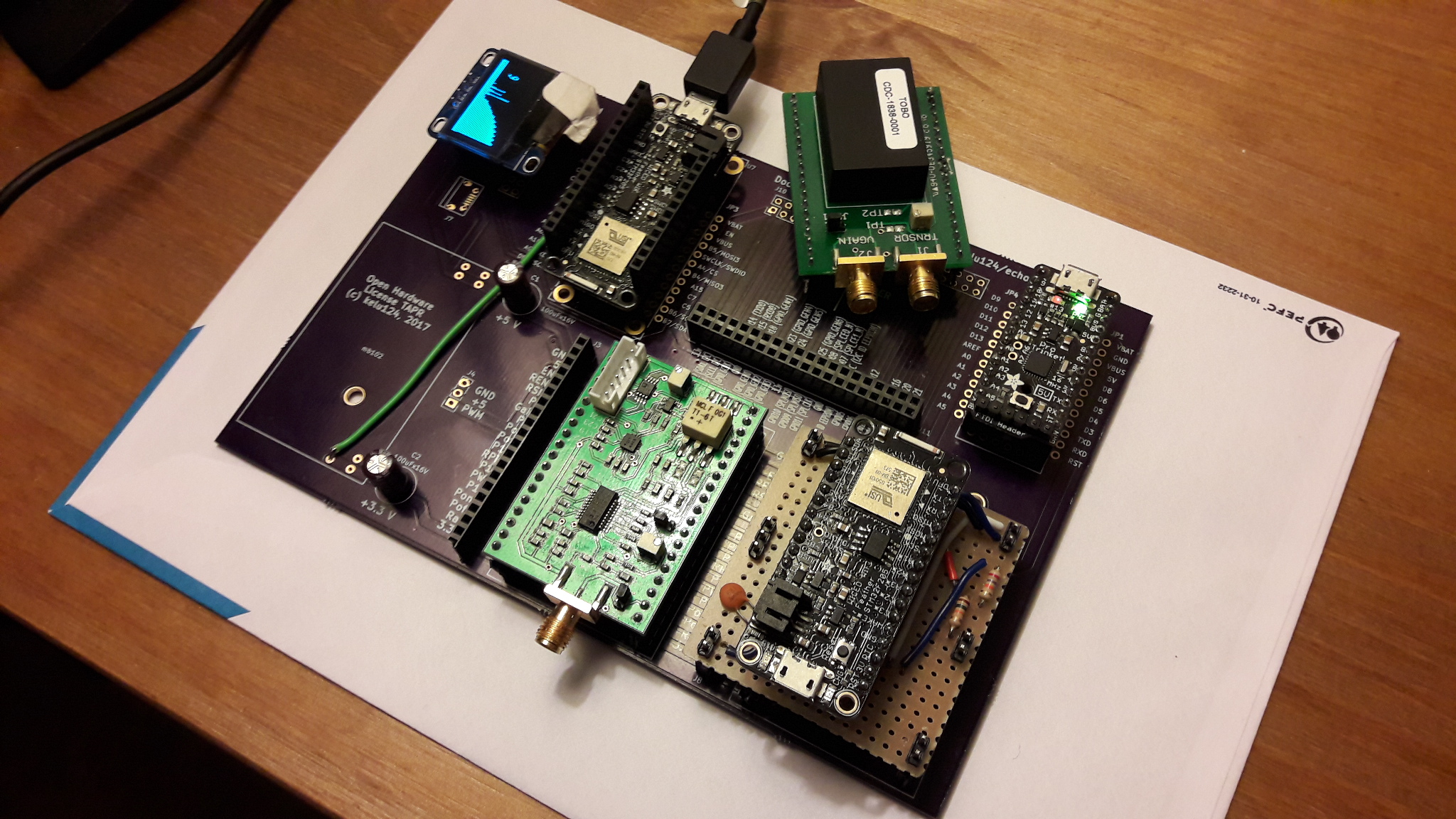
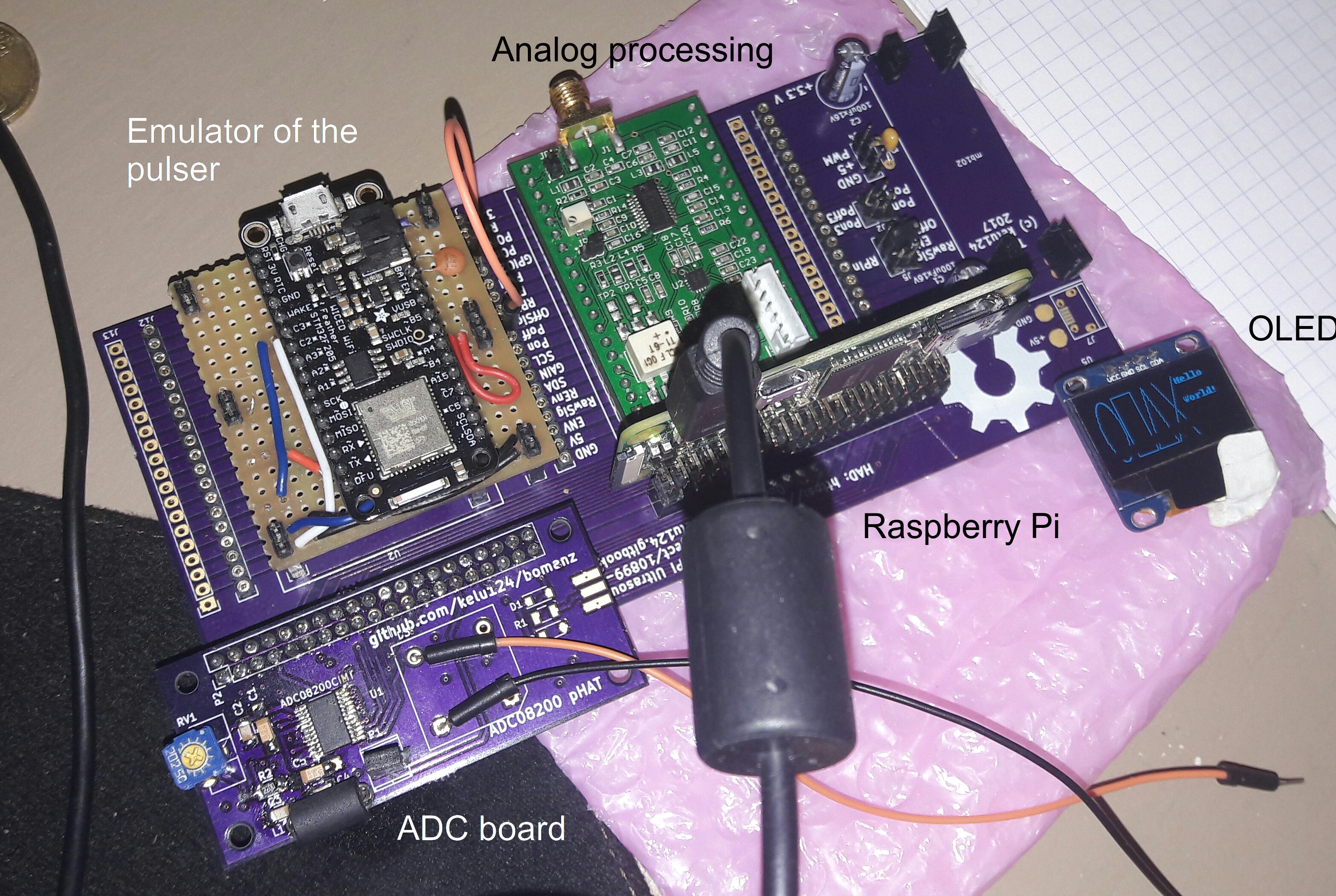
This kit consists of several modules mainly built from easily available components - after a short benchmark of existing ICs. Two electronic modules were specifically designed to provide the basic development kit.
- the Transducer Pulser Module (TPM): designed to provide a precise high-voltage pulse, necessary to excite the sensor, while remaining robust enough to be controlled by an Arduino;
- the Analog Processing Module (APM): designed to correctly process the raw ultrasound electric signal, while easily exposing all intermediary signals, and exposing a digital output to the user
- the RPi high-speed ADC uses two interleaved AD9200, clocked with the RPi, which reads at 11Msps, leading to an effective 22Msps acquisition speed (bottleneck being the RPi copying the ADC values through the GPIOs register to RAM). The signals can be read as is (eg in case of analog enveloppe detection) or offset by Vref/2 (to acquire the raw signal). Due to the GPIO necessary to run the modules, we are left with 2x9 GPIO left, resulting in a 22Msps, 9 bit ADC. One or two logic signals can additionaly be sampled - for an external motor hall sensor for example.
A modular approach was chosen to ensure that each key component inside the ultrasound image processing can easily be replaced and compared with another module. Each electronic module takes the place of a function in the signal processing chain or allows tapping into the different signals circulating between the blocks.
Previous experiments have been done, to get images using different digital acquisition systems, such as a bitscope, a STM32, or a high-speed ADC for beaglebone. The Raspberry Pi was retained in the end for its ease of use, its price, and community working on it - increasing the potential reach of the project.
Assembly guide
Required materials
- A pulser board - to generate the high voltage pulse to use the transducer
- An analog front end - to amplify the weak signals generated by the echoes
- an ADC cape - a custom made 11Msps to 22Msps ADC pHAT for Raspberries.
- a Raspberry Pi, 0 or W to manage everything
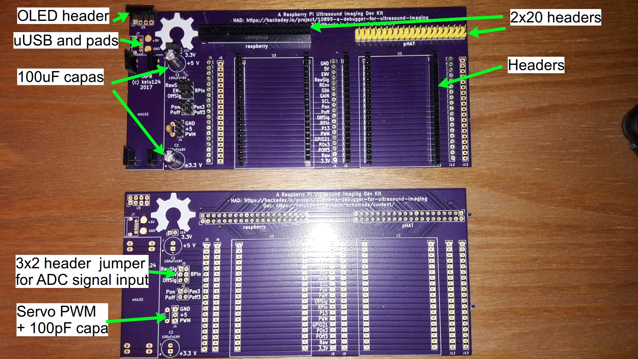
- the motherboard, v2 - to connect the different modules together
- and some extras such as headers, jumpers, and a smallish OLED screen
For the transducer, one can use either a ATL mechanical probe for example, or a piezo + servo setup, to mechanically scan the medium to be imaged
Quickstart of the Pulser module
The pulser module
The assembly is detailed below:
Read more on the dedicated page.
Controlling the pulser
The pulser is controled by a double signal, one, PulseOn, to start the pulse, and the other, PulseOff, to bring the pulse back to 0.
Note: The setup presented here was with the Raspberry Pi + ADC setup. Raspberry Pi kernel modules and software can be found following the previous link.
The PulseOn, PulseOff and signal output are represented below.
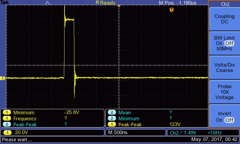
Calibration and tests
Yellow is PulseOn, Blue is PulseOff. The logic is also 3.3V and 5V tolerant. Here, the control signals were produced with a raspberry pi.
For the sake of testing, keep PulseOn as long as your pulse needs to be, but keep PulseOff (or "Damper") on for something around 5 - 10 us. You can test for example with the simple code here, inspired from the retired pulse control OneEye.
Controls
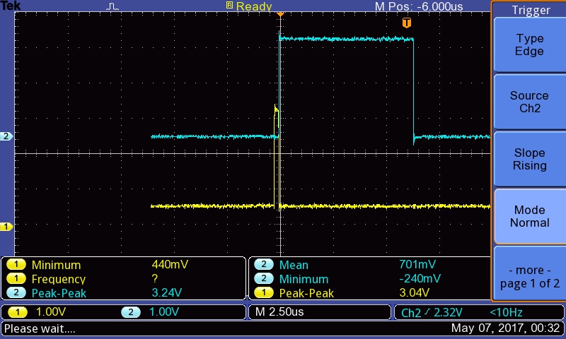
Output on the pulser SMA to transducer
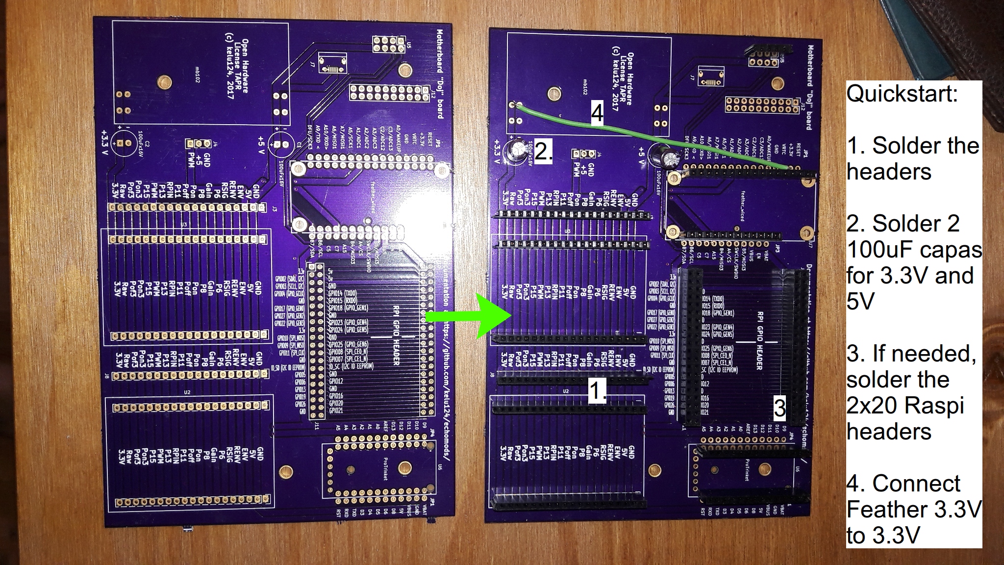
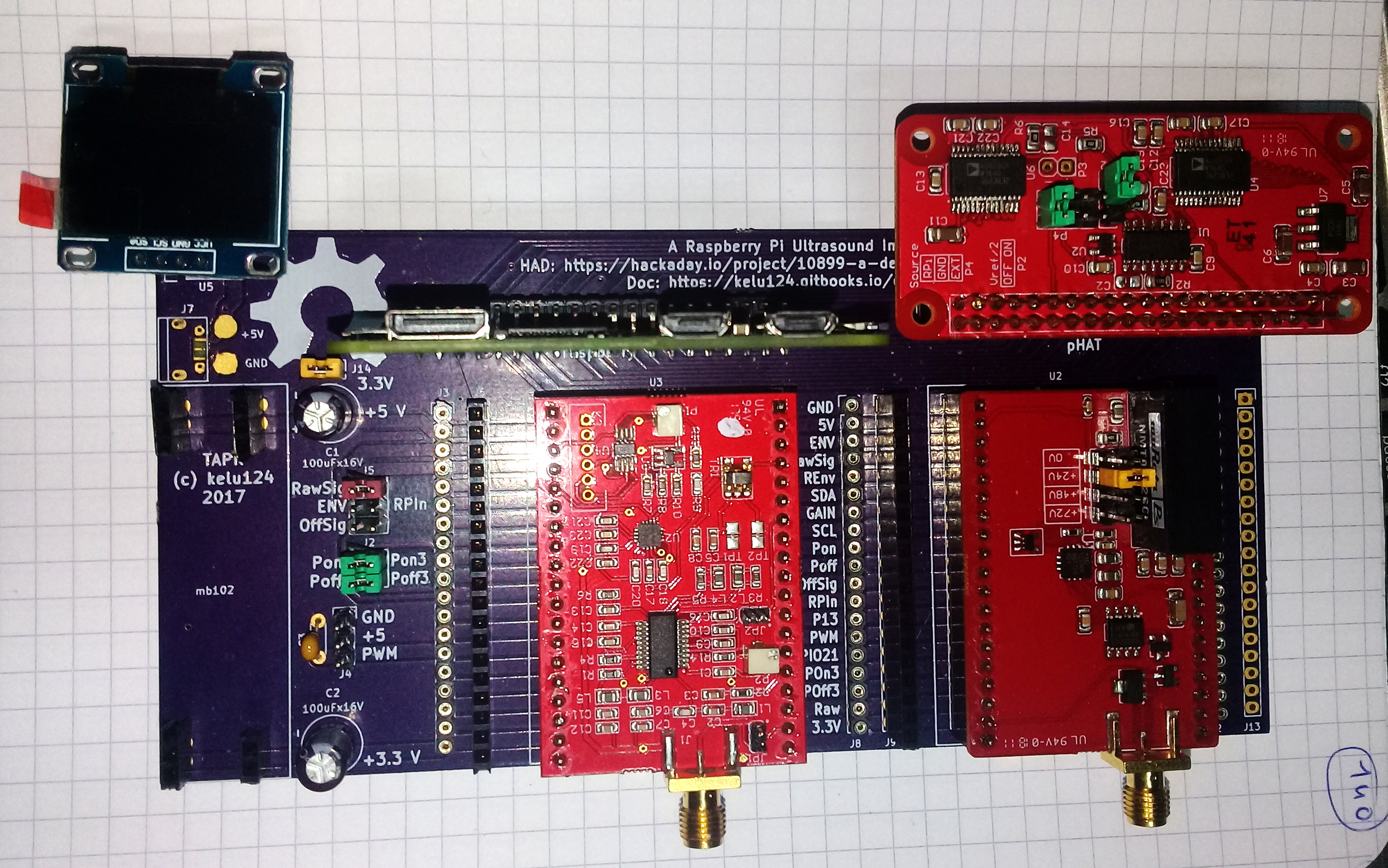
Quickstart of the mother board
BEWARE !!
As a piece of advice, don't solder your modules directly on the motherboard... unless you're sure that they are properly set up, that there's no short, ... and keep the design as modular as possible.
Instead, solder header, 19 slot long, for each side of the modules. These will be the host for the pins coming from the different modules.
Nothing can keep you from soldering round slot headers for ease of using wire jumpers.
Don't forget to put some capacitance on the dedicated slots on the motherboard to smooth the supply - and on Doj v2, to include the 3.3V jumper (above the 5V capa) so that the Pi can provide the necessary 3.3V to the board, and, if using a Pi, to solder the Pon <-> Pon3 and Poff <-> Poff3 if you want to use a pulser at 3.3V from the Pi.
Doj v1.2
The PCB can be ordered on OSHPark - or ask me if I have one available (maybe check on Tindie)
How to solder the PCB ?
Example of Doj v2 powered through Raspberry USB
Doj v2
The PCB can be ordered on OSHPark - or ask me if I have one available.
How to solder the PCB ?
Example of Doj v2 powered through the Feather module
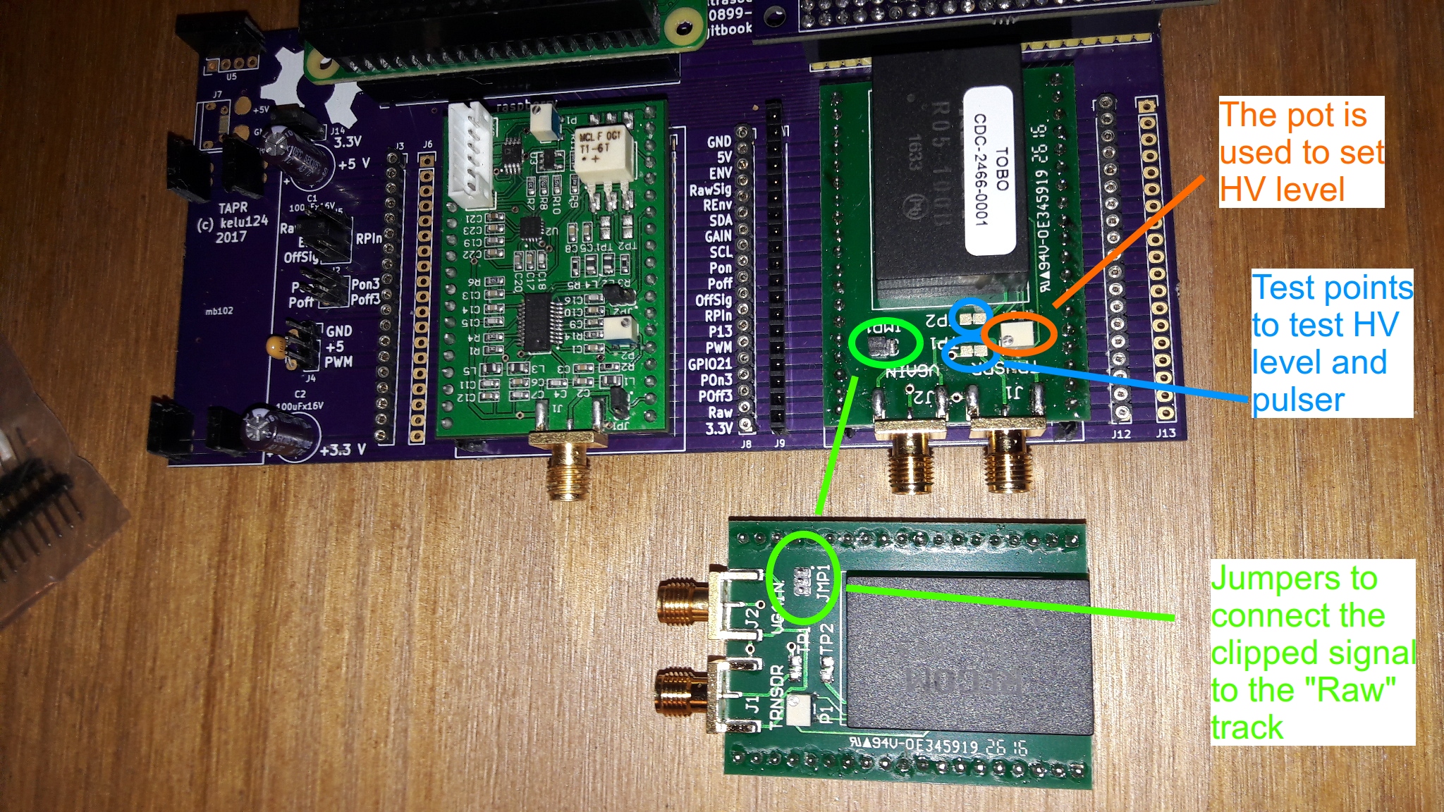
Quickstart of the APM module
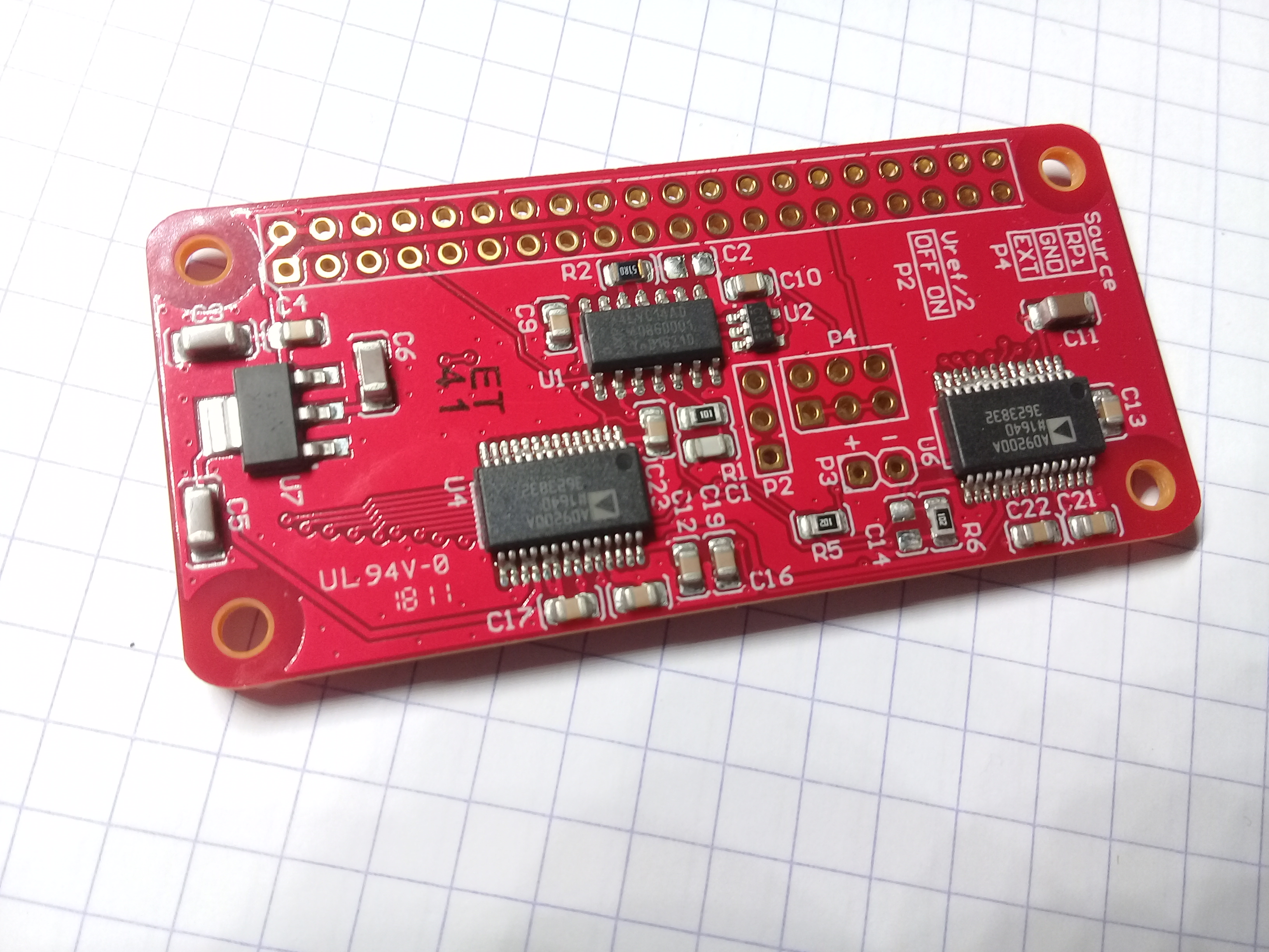
The Analog Processing Board module
The assembly is detailed below:
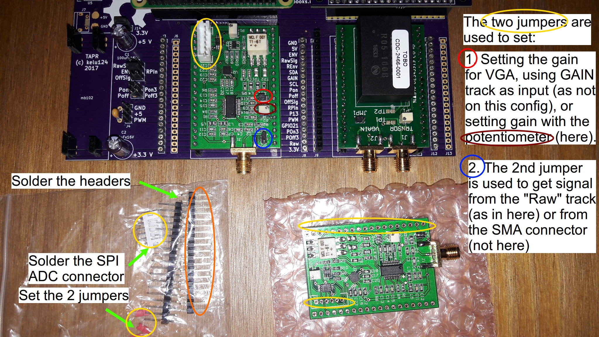
Specific points:
- A couple of headers to solder.
- Don't bother soldering SPI (the white header) if you don't plan on using it
- Setup the small jumper (in blue) to get signal from the "Raw Track". Other position is to get signal from SMA. Beware, there's no signal clipping there on this board.
- Setup the small jumper (in red) to get constant gain for TGC from the pot circle in dark red. The other position can be used if you plan on using the "GAIN" track (between 0 to 1V) to control the gain.
Read more on the dedicated page.
Testing and calibrating Tobo
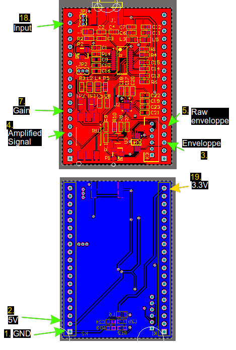
You need to power Tobo with a 3.3V source on track 19, and 5V on track 2.
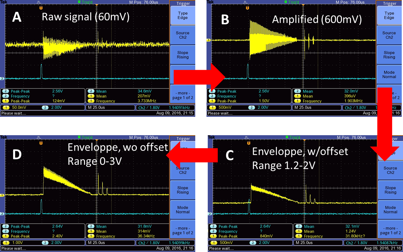
Apply a small voltage on Raw Track with jumpers rightly positioned (A). You should get a amplified signal on track RawSig (B), the offset enveloppe on REnv track (C), and envelopped of the signal on
BEWARE! Only apply small voltages to input (less than 1 Vpp ideally, here calibration was done with 60mVpp signals)
If not using a motherboard, connections are detailed below:
Quickstart of the ADC module
Hardware steps
For the motherboard PCB based solution...
Just plug it into the board!
Beware of the headers! The idea is to have connections between the board and the pHAT. You can use any type of headers =)
For a standalone version
- The ADC onboard selector (3x2) enables one to check input, either through the RPi pin, or the onboard entry.
- the 3x1 jumper allows one to offset a 0-centered signal to have an offset of vRef/2 (ie the zero will go to the middle of the range)
The ADC module
You can use the standalone SD card image. Alternatively, you can setup the development environment as described below.
The standard module code is here and can be compiled using these steps.
The full procedures are described at on the raspberry doc page
Log now on this raspberry, and run the run.sh command to load the driver of the ADC. You'll see that the module appears as a /dev/hsdk device.
Capture occurs with a
cat /dev/hsdk > myfilename.dat
Then copy the newly created file on your PC or where you need it. It dumps the raw GPIOs signals as described here
Beware! If you want to get a signal between [-1.5V and 1.5V], consider using a in series with input to remove all DC bias, and make sure the jumper are set as in the images above.