Goblin: a TGC-Envelop-ADC module
What does it look like?
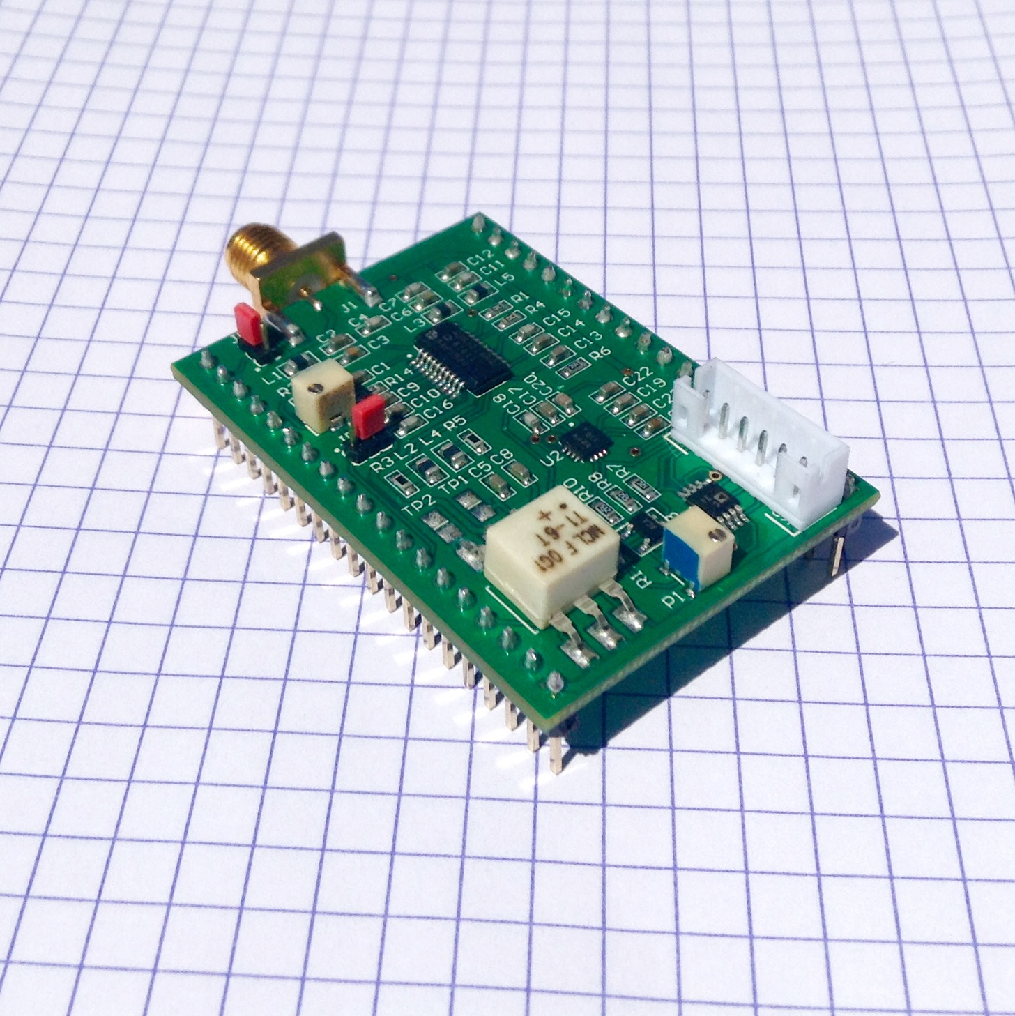
Information
What is it supposed to do?
The aim of this echOmod is to get the signal coming back from a transducer, and to deliver the signal, analogically processed, with all steps accessible to hackers.
With more details, this Goblin board aims at getting a signal, and giving access to key points within the signal processing chain for ultrasound imaging, namely:
- Getting access to a TGC
- Getting the enveloppe of the signal
- Cleaning the signal before feeding in the on-board SPI ADC
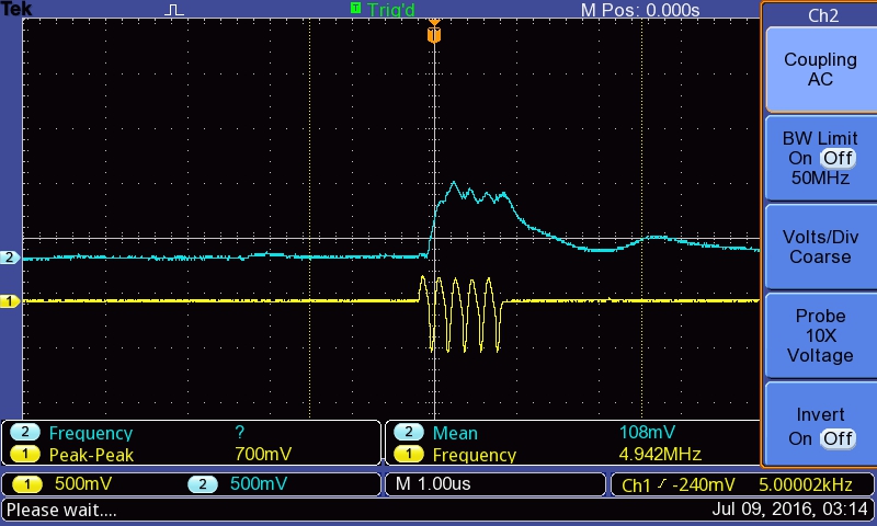
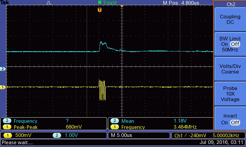
All key signals are accessible, and jumpers, as well as pots, enable on-board fine-tuning of the signals. See more details on the testing session, to see the behavior of the board on a oscillo.
It's also a first try at a SPI ADC. Using a up to 3 Msps one in order to catch only the enveloppe, to be tested with other uC, RPi or BBB. Test have been also done with 6MSps, arduino IDE-compatible, STM32.
How does it work: block diagram
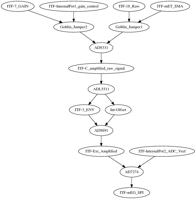
ITF-7_GAIN->Goblin_Jumper2->AD8331->ITF-C_amplified_raw_signal->ADL5511->ITF-3_ENV->AD8691->ITF-Ext_Amplified->AD7274->ITF-mEG_SPIITF-18_Raw->Goblin_Jumper1->AD8331ITF-mET_SMA->Goblin_Jumper1ITF-InternalPot1_gain_control->Goblin_Jumper2ITF-InternalPot2_ADC_Vref->AD7274ADL5511->Int-Offset->AD8691
This can be summarized below - all the signals represented are accessible via separate on-board pins:
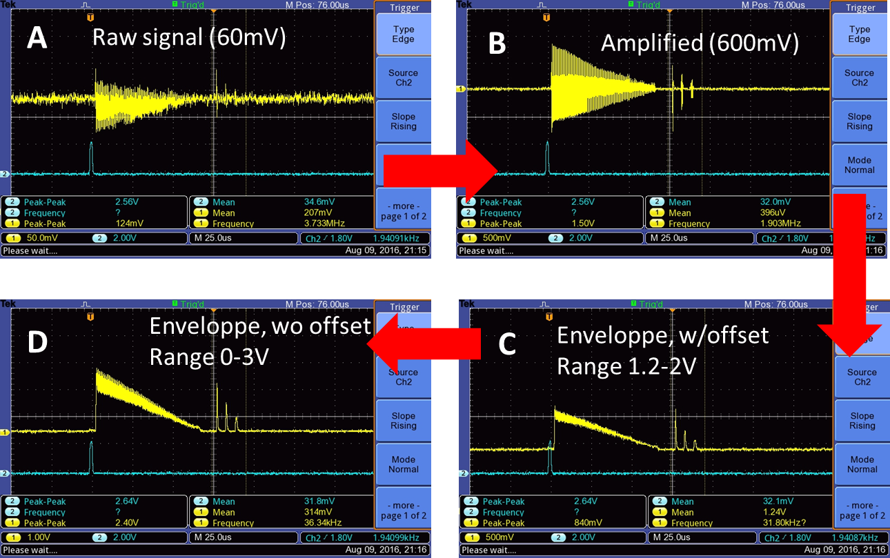
Input/Output:
About the module
Pros
- Only needs 5V and 3.3V inputs.
- Energy use is relatively low: at 9V, Tobo, Goblin, and a trinket pro ask for 180mA.
- ADC V_REF is flexible: better resolution in output of the ADC
- E_REF is being removed from the signal output, better than Murgen, where we lost 1.1V from the signal range.
- ADC is http://fr.farnell.com/jst-japan-solderless-terminals/b6b-ph-k-s-lf-sn/embase-entree-sup-6-voies/dp/9492453?MER=sy-me-pd-mi-alte -- what appropriate connector ? http://fr.farnell.com/jst-japan-solderless-terminals/vhr-6n/boitier-connecteur-rcpt-6pos-1/dp/2399220 ?
Cons: what to to make better
- Takes a lot of space because of the modularity. Jumpers and pots could be removed, not to mention SMA.
- The amplifier removing E_REF brings in some noise: a filter could be used there to remove to high frequencies.
- The SMA brings little, but still a noise analysis could be done to assess the difference between routing the signal through a SMA cable or through the pins.
- There are only two layers. A fourth one to connect each pin to the other pin on the same row, as well as a ground plane, could help with the noise.
- Little flexibility from the use of ICs - but sufficient of sorts for our use.
- The ADC is borderline in terms of speed of use. A higher sampling rate could be useful.
- There was a bug with the ADL5511: need to know how it shuts down.
Detailed view
BEWARE
The transfo has been updated (see this folder for a version with an easily found transfo - untested yet).
Explained
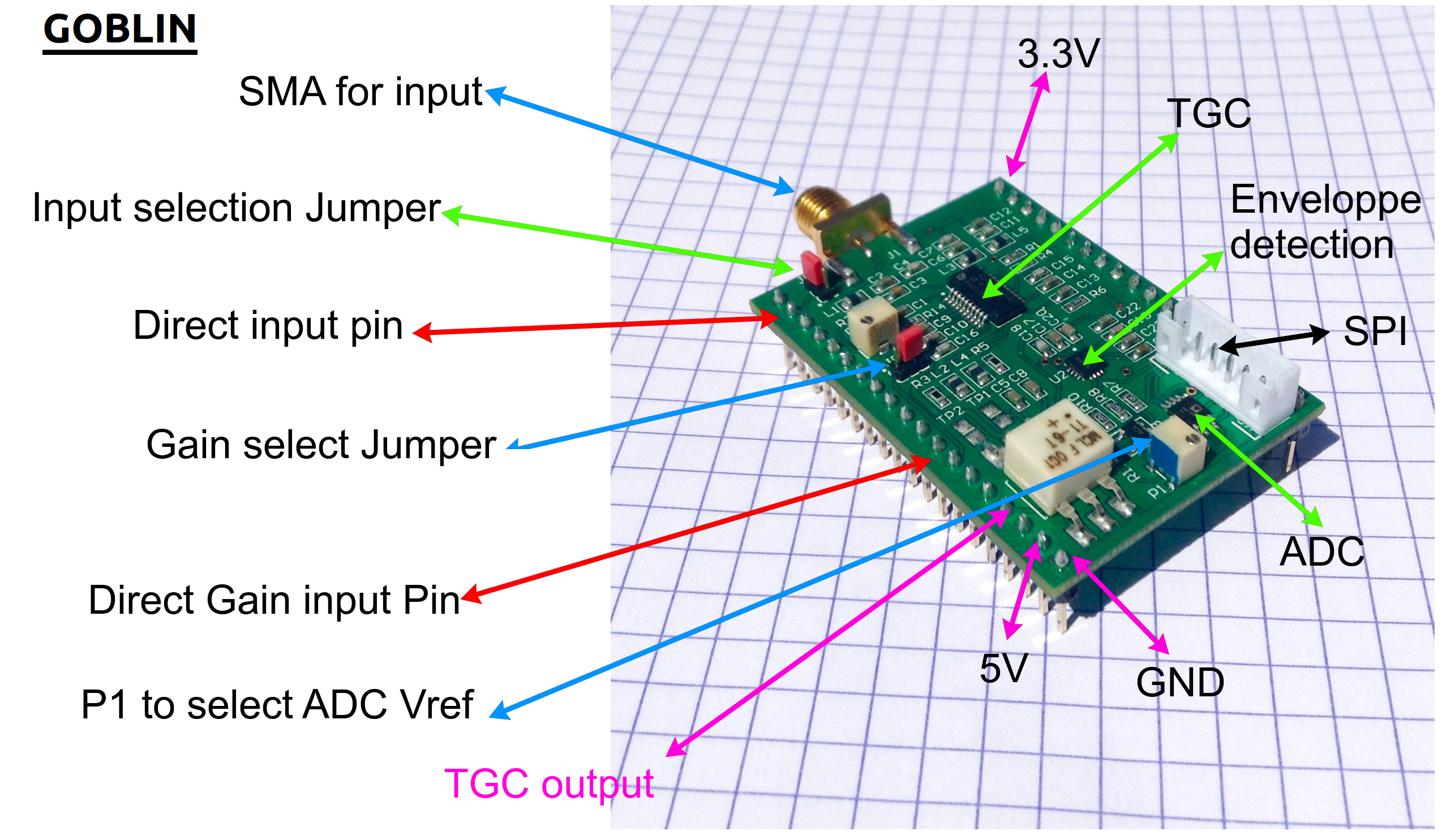
In/Out
See more details of the acquisition of in/out of the module, using the PRUDAQ Module.
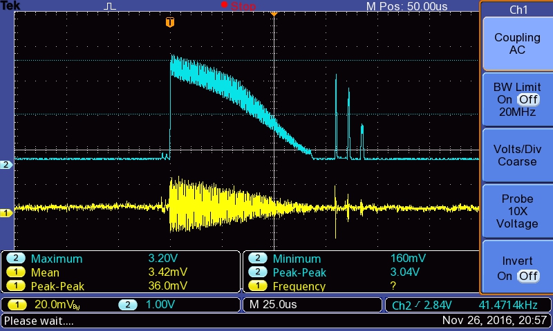
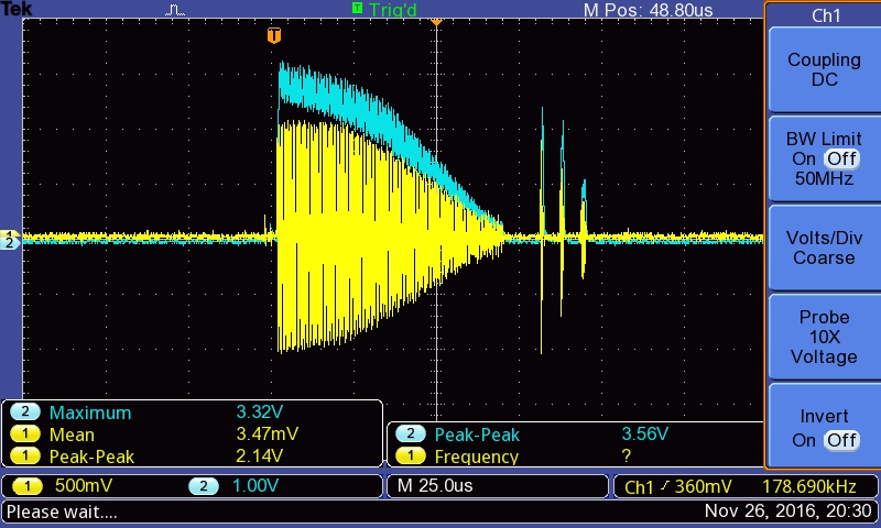
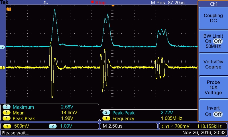
Comparing the signals: amplified signal vs enveloppe detected
The overall signal
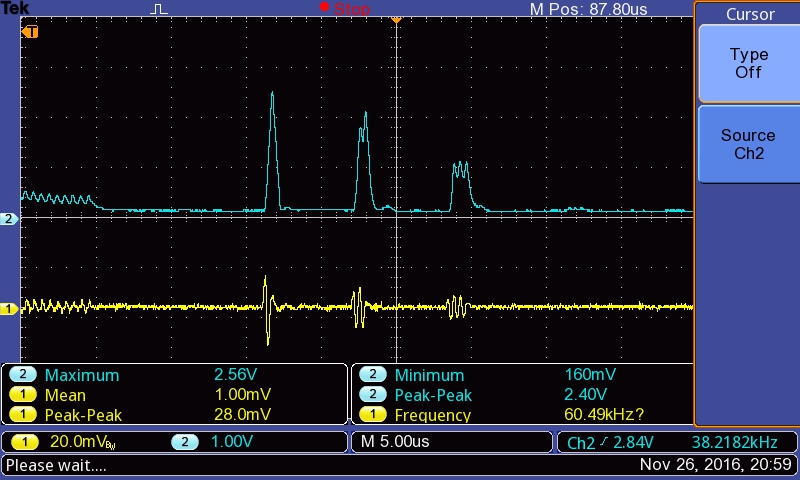
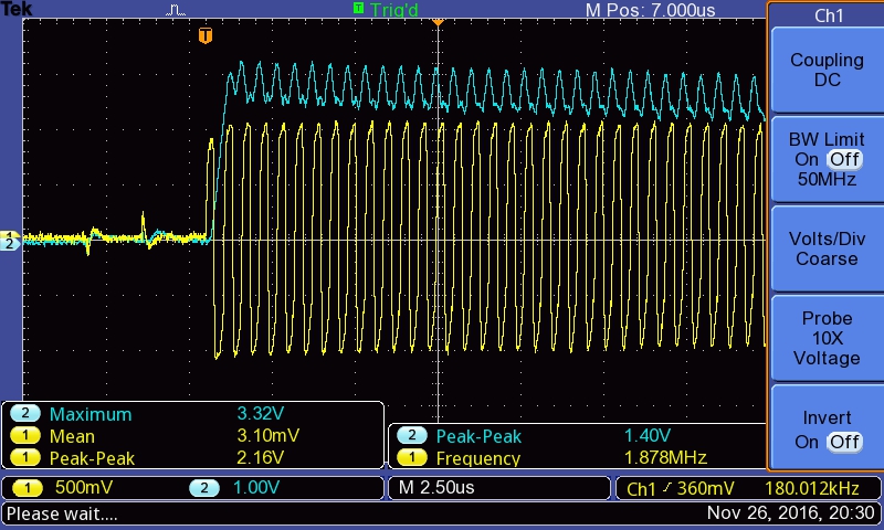
Details
Details on the peaks
Schematics
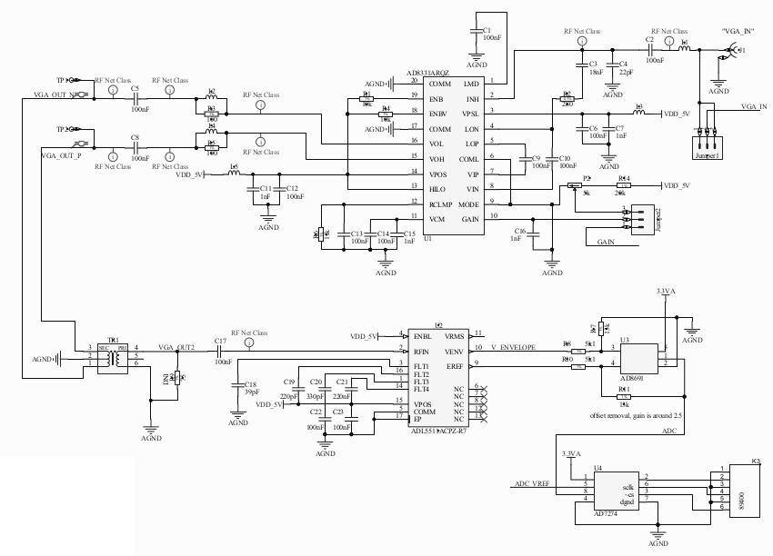
Constraint and limits
Tests
Access to raw data
Data sampled at 10Msps on the PRUDAQ on both channels.
See the Jupyter notebook In-Out.ipynb
Data is saved here. It's 32Mb of sampling at 10 Msps. Full repo for the measure test. Let's check the Signal In vs Signal Out:
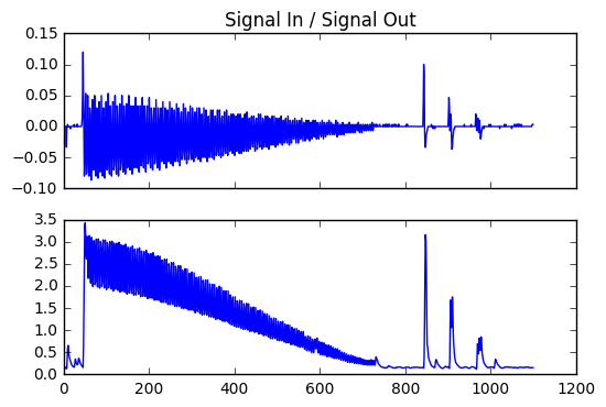
with details:
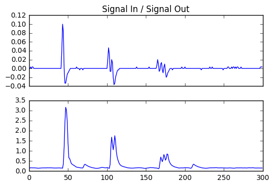
Trying with different frequencies
At 3 MHz
At 5MHz
At 7.5MHz
At 10MHz
Difference between enveloppe and ADC input?
-> the offset is removed, there's also a small gain (x2).
See below: there's an offset at the enveloppe detection (~RMS), which is removed. Enveloppe is 500mV before, comes at 1V+ afterwards.
Before the AOP
After the AOP
Idea for onboard ADC
The AD7273/AD7274 are high speed, low power, 10-/12-bit, single supply ADCs, respectively. The parts can be operated from a 2.35 V to 3.6 V supply. When operated from any supply voltage within this range, the AD7273/AD7274 are capable of throughput rates of 3 MSPS when provided with a 48 MHz clock.
Discussions
TODO
- Test Goblin v2
DONE
- Check the power consumption
- Testing the in and out signals of the board with the prudaq.
- Specs to write
- Agreeing on the strips
- Check if 5V and 3.3V are stable
- Defining the ICs to use
- Getting schematics
- Send microcircuits to Edgeflex
- Receive the module
- Publish the sources in KiCAD (@Sofian maybe?)
- CANCELLED - Test it with the EMW3165
- Plug it to a RPi0 or BBB or STM32
- Connect the ADC to a RPi0
People
- Sofian (for preparing the field with Murgen)
- Vlad for his expertise with Altium
