Using a dual ADC raspberry pHAT for 20Msps+ acquisition
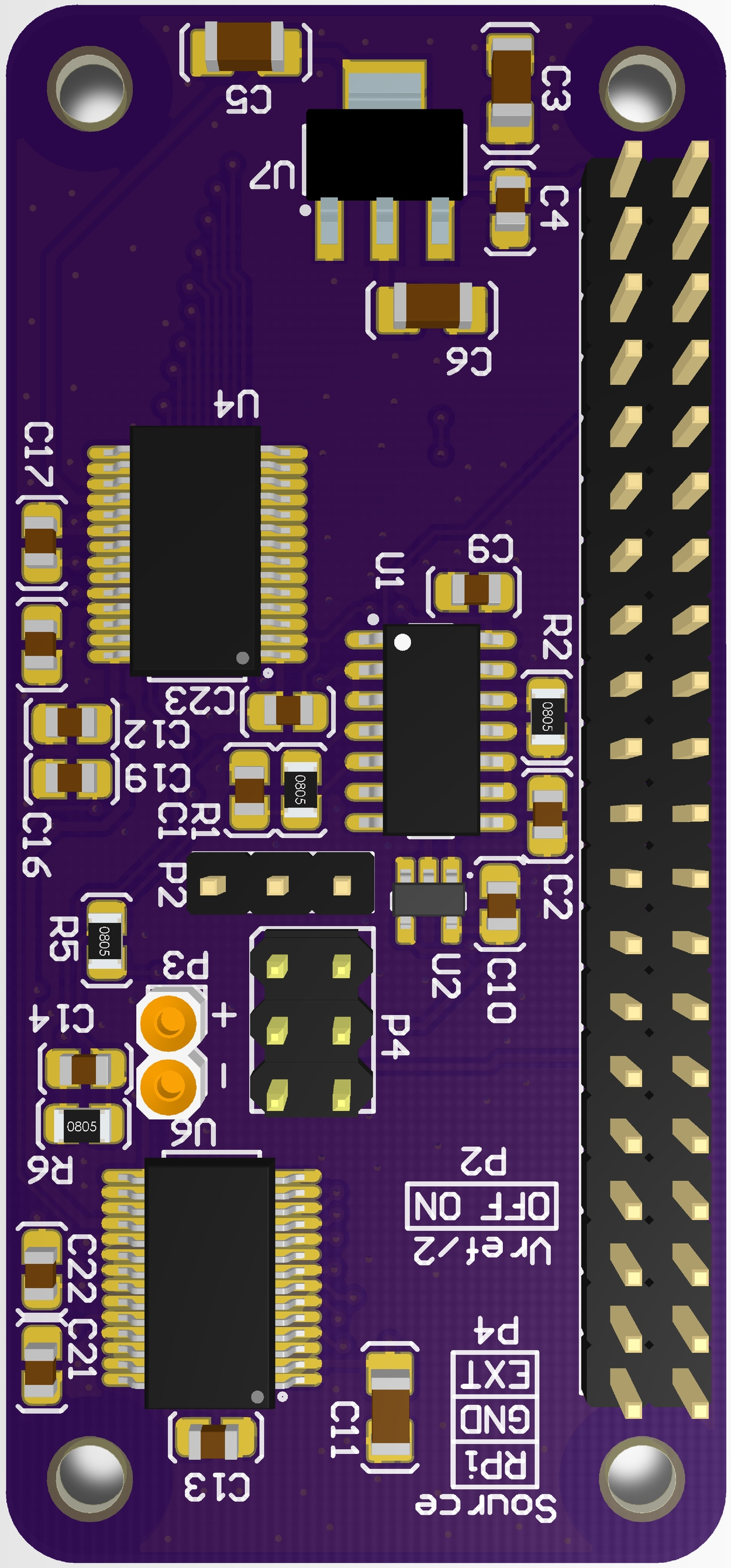
What does it look like?
Information
What is it supposed to do?
The aim of this module is to achieve 20Msps, at 9bits or more.
How does it work: block diagram
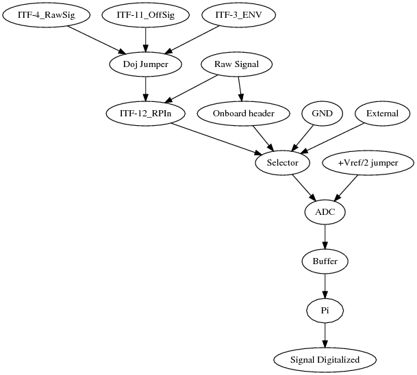
Raw Signal->ITF-12_RPIn->Selector->ADC->Buffer->Pi->Signal DigitalizedRaw Signal->Onboard header->Selector+Vref/2 jumper->ADCGND->SelectorExternal->SelectorITF-4_RawSig->Doj Jumper->ITF-12_RPInITF-11_OffSig->Doj JumperITF-3_ENV->Doj Jumper
About the module
Pros
- High speed, 9 bit ADCs!
- Full Altium source, Gerbers, BOM, schematics.
- Driver for the board.
Cons
- SMDs is tough to assemble
- Linux is not real time: there will be inaccuracies in the measurements!
- Need a custom kernel module
Constraint and limits
- See above ;)
Discussions
Where can I get elements to play with ?
You can refer to the 20180415r experiment. It is made of a unipolar pulser, double ADC board, and analog processing board. The experiment documentations is based on :
- Raspberry Pi drivers which create the /dev/ device on the raspberry pi from which a
cat /dev/hsdk/ > Datafile.DATextracts signals. The driver includes control for the pulser. - An example of Raw data that is created out of the driver
- the Jupyter notebook which processes capture files from the ADC into signals
- the resulting Processed data
Even without the board, you can use an example of such a file to play with.
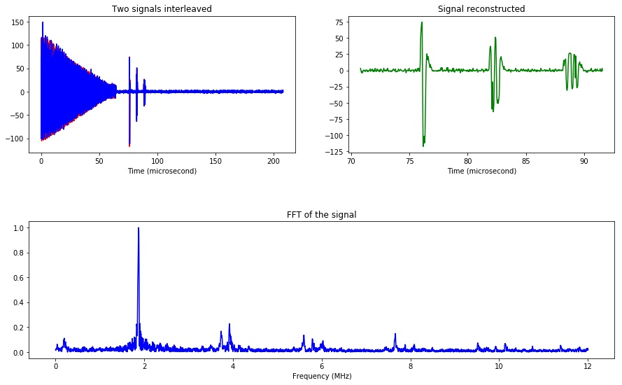
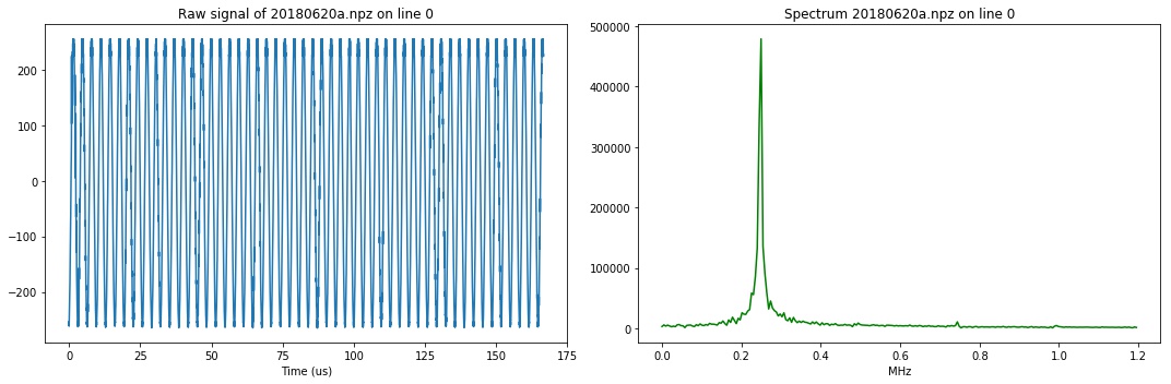
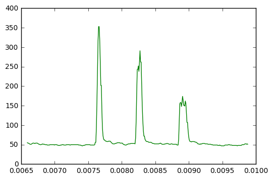
Let's start with the end: it works!
Testing the module with the signal emulator module, which yields a signal at 1.9MHz, it well seen at 1.9MHz, with a sampling speed equal to two times this freq, ie 24Msps ! See the details below:
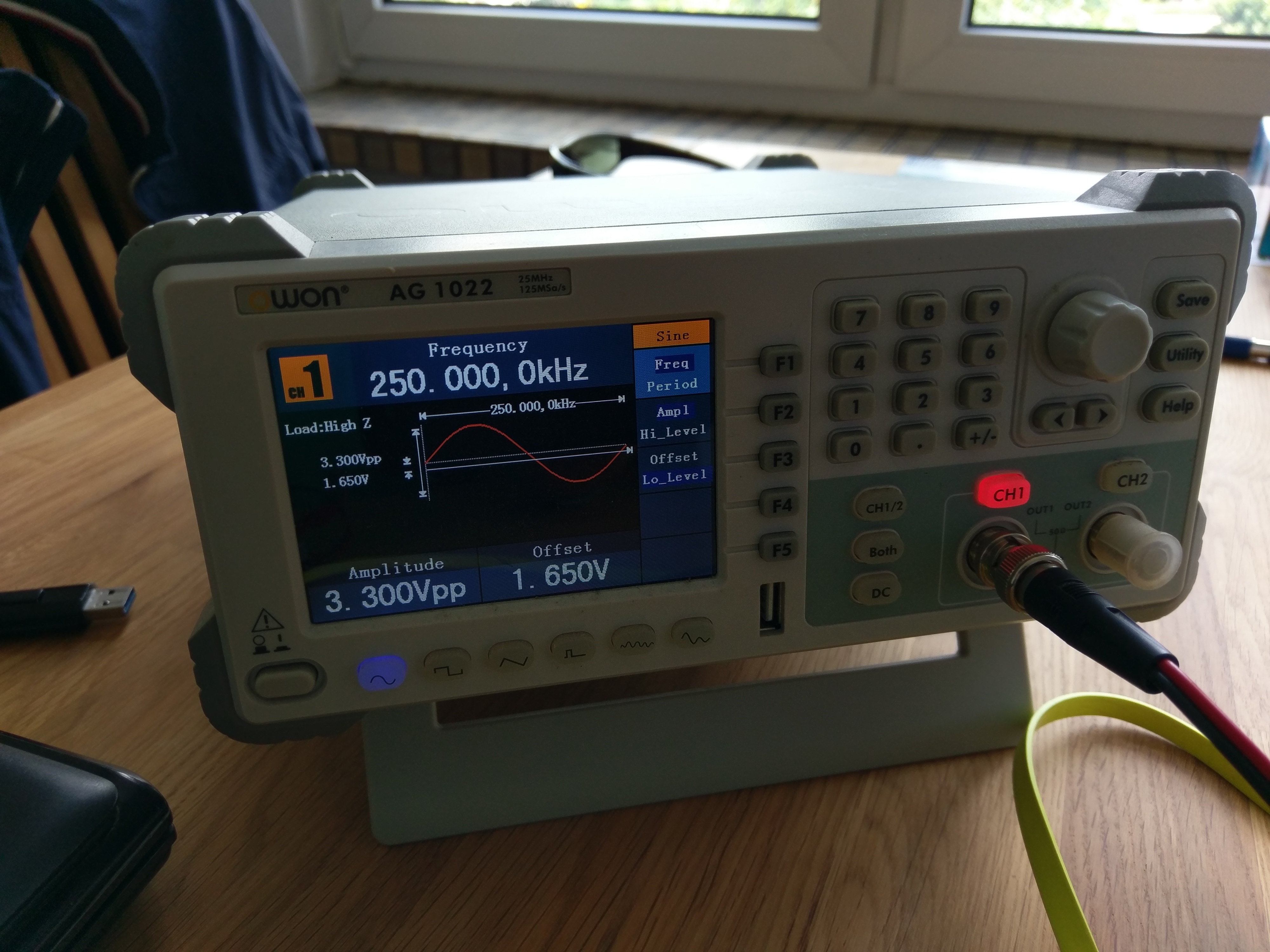
Test at 250kHz
Experiment is detailed here.
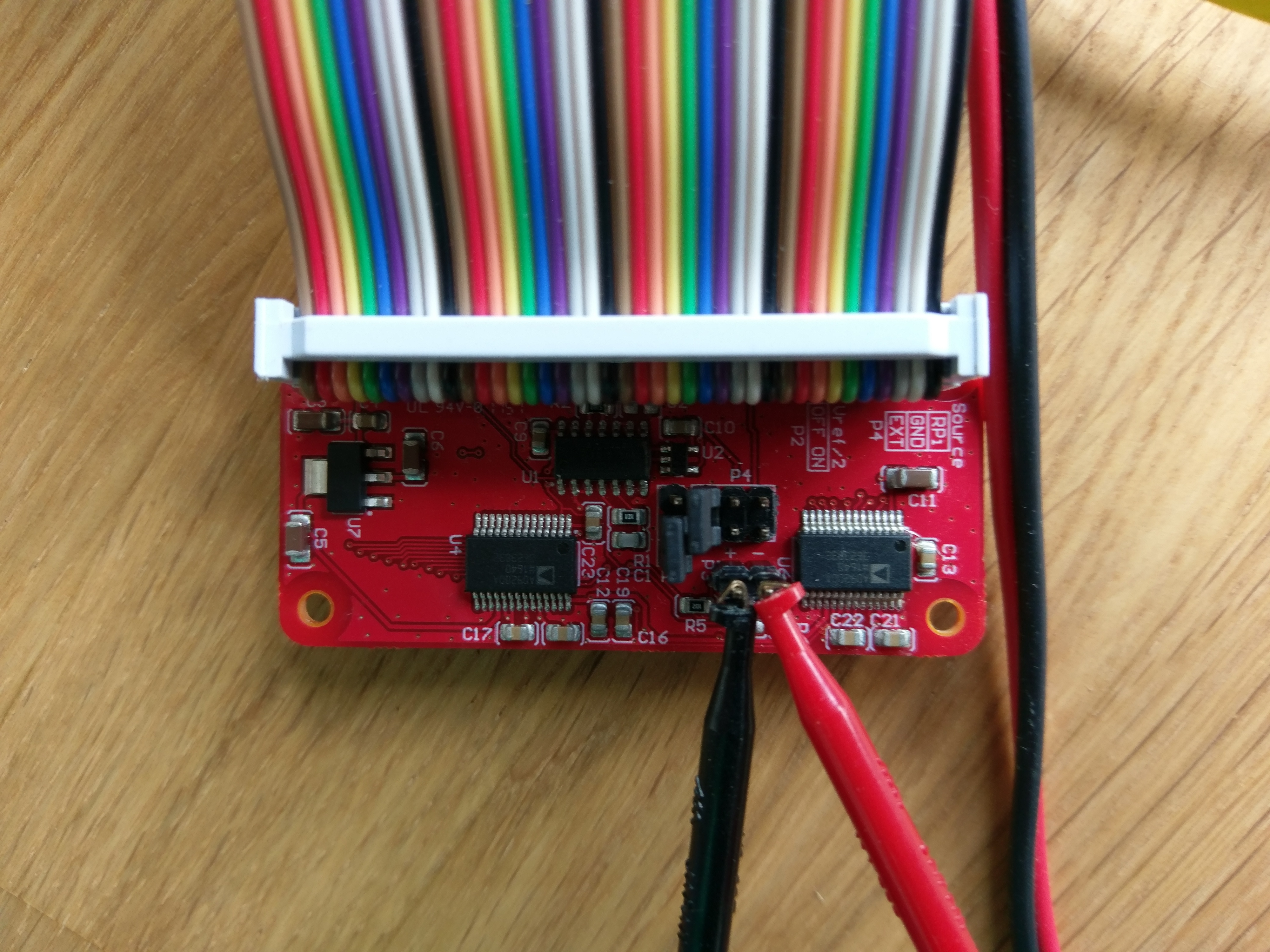
Signal generator sent to the pHAT
Connected to the ADC, then to a RPi through a ribbon
Results
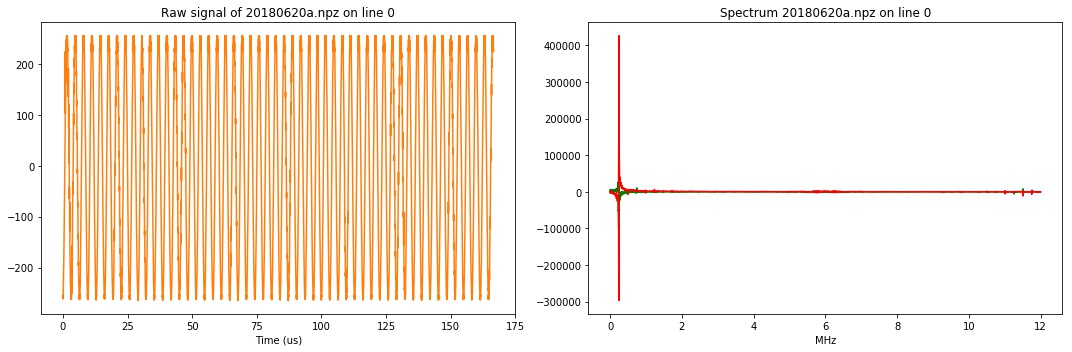
With the details
Problem and solution
Problem was that the Pi0 or PiW, with the current kernel module, can't run faster than around 10 to 12 Msps. Clock can be faster, but the memcpy limits the transfer to memory. Soooo.. what can we do? As a reminder, I wanted at least a 10Msps 10bit ADC.
Solution Why not interleaving two ADCs, with clocks in opposite phase? Hum that means 2 times 10 bits, and I had only 18 pins left once the Ultrasound SDK board connected. That means.. quite obviously, 2 times 9 bits.
So now I can run at twice the speed of the transfer, so a bit over 20Msps, over this time 9 bits. Or by oversampling, that could be 10Msps at 10 bits. With more flexibility !
Win.
At least for the moment, now I need to order the PCBs and some components.
-> BOM is around 30$ components, 5$ OSHPark PCB.. that's quite neat.
Raw signal acquisition and enveloppe with this ADC pHAT
With the enveloppe
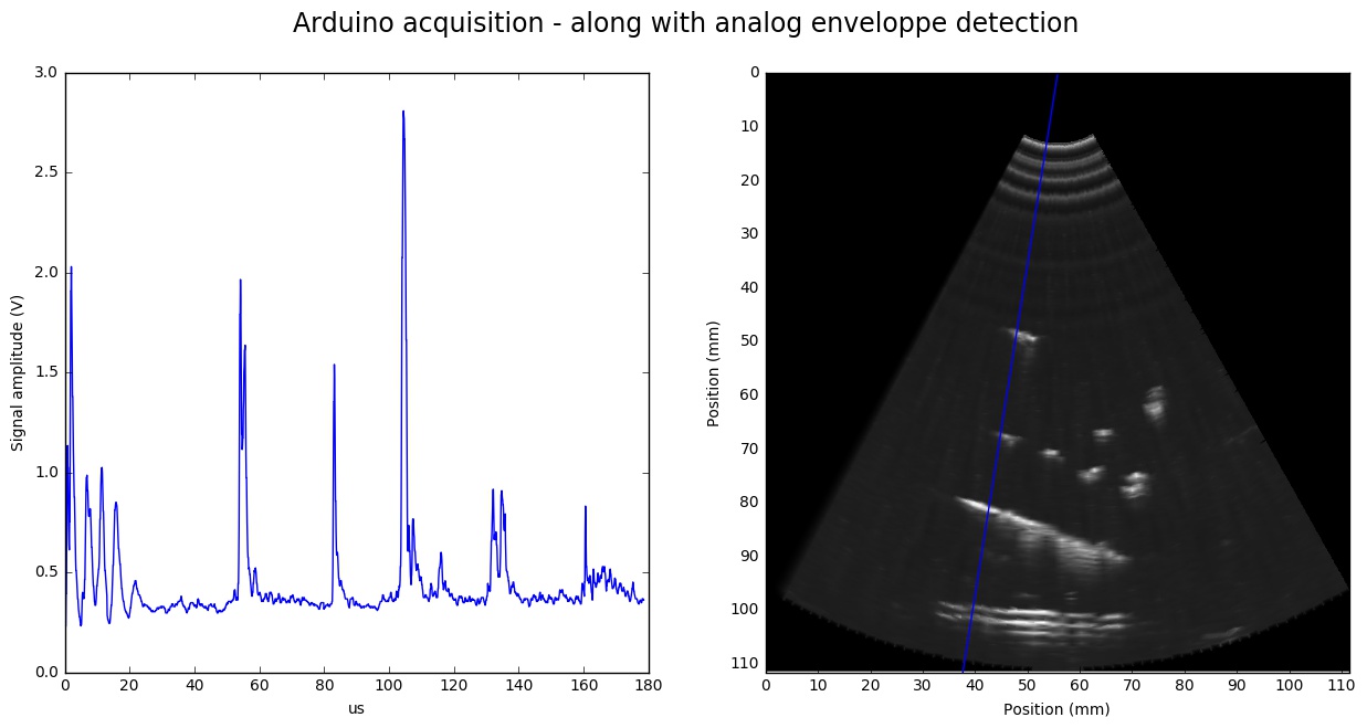
With the raw signal
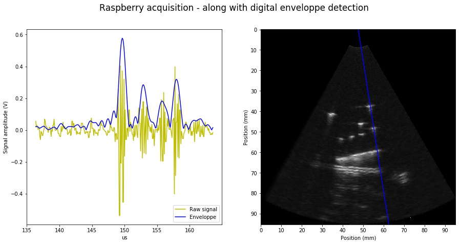
First acquisitions:
See the jupyter notebook:
Issues: bugs in connected ADC pins + no offset really
What does it look like ?
Without headers
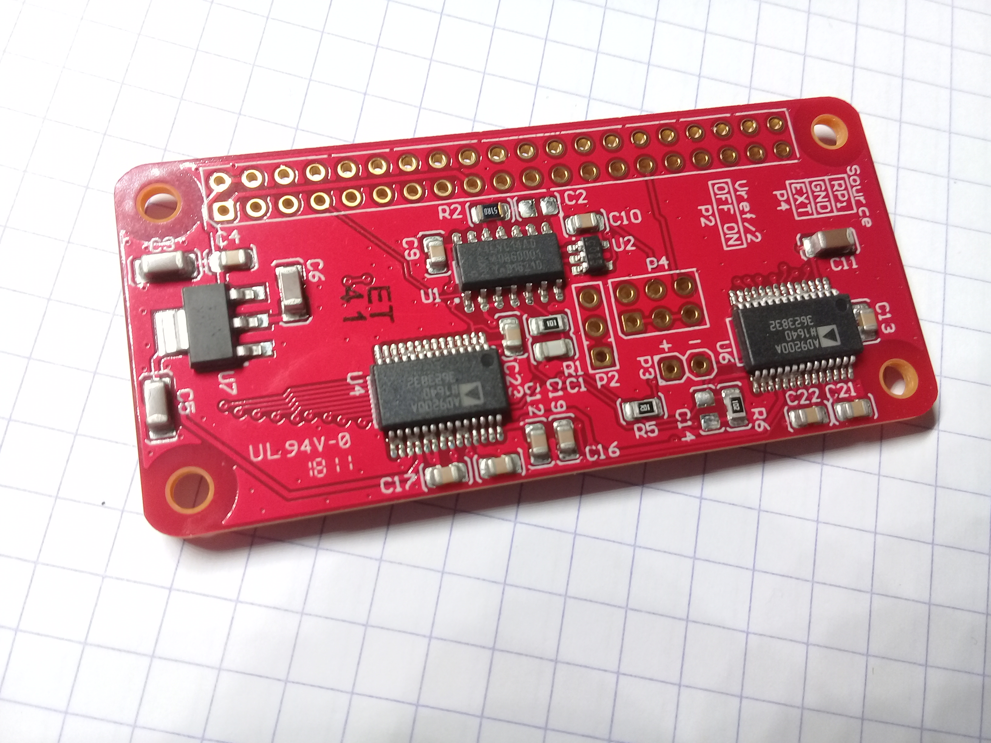
and the corresponding schematics (PDF).
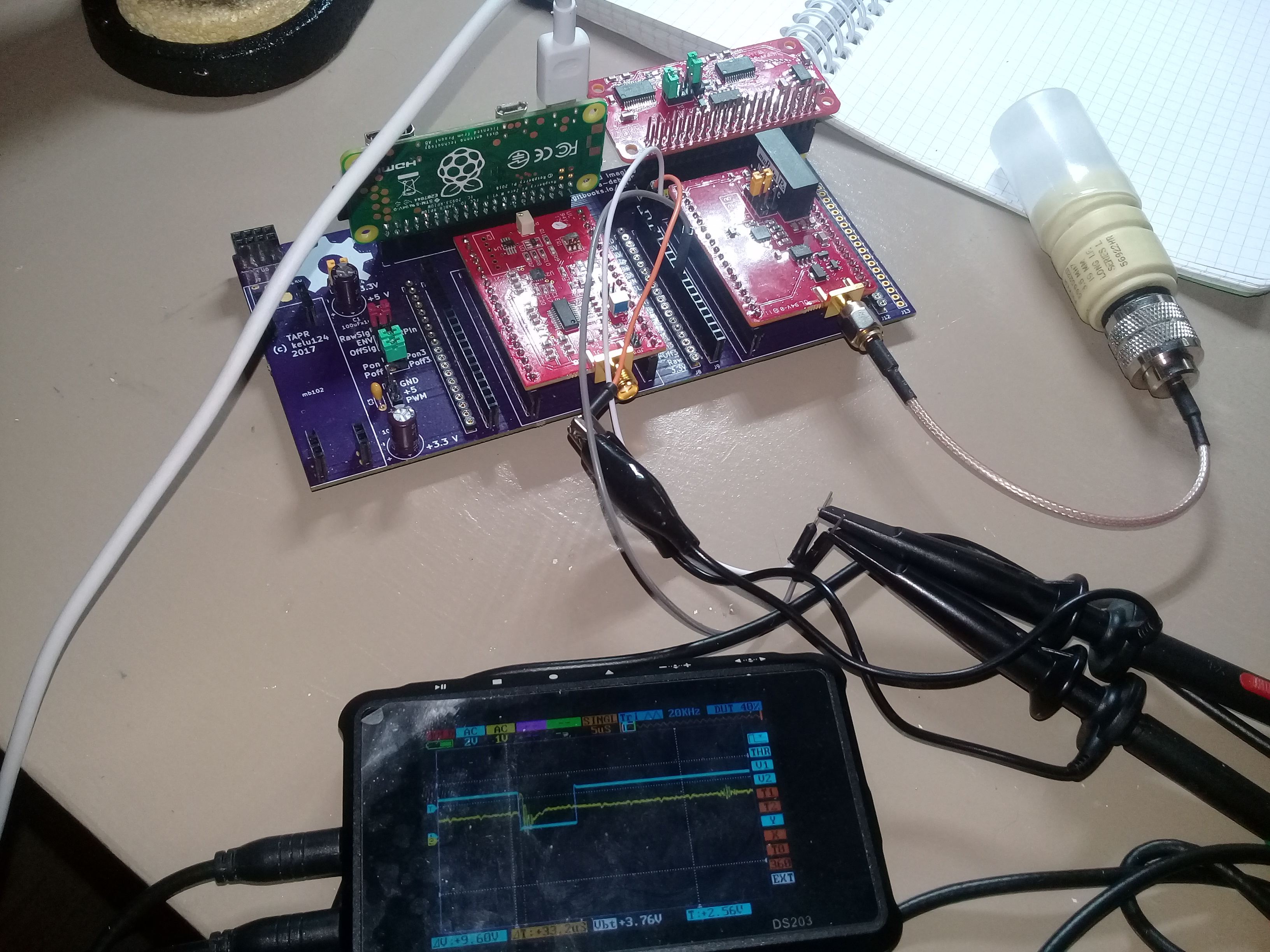
On the motherboard
Beware the motherboard is designed to have the phat assembled as shown below
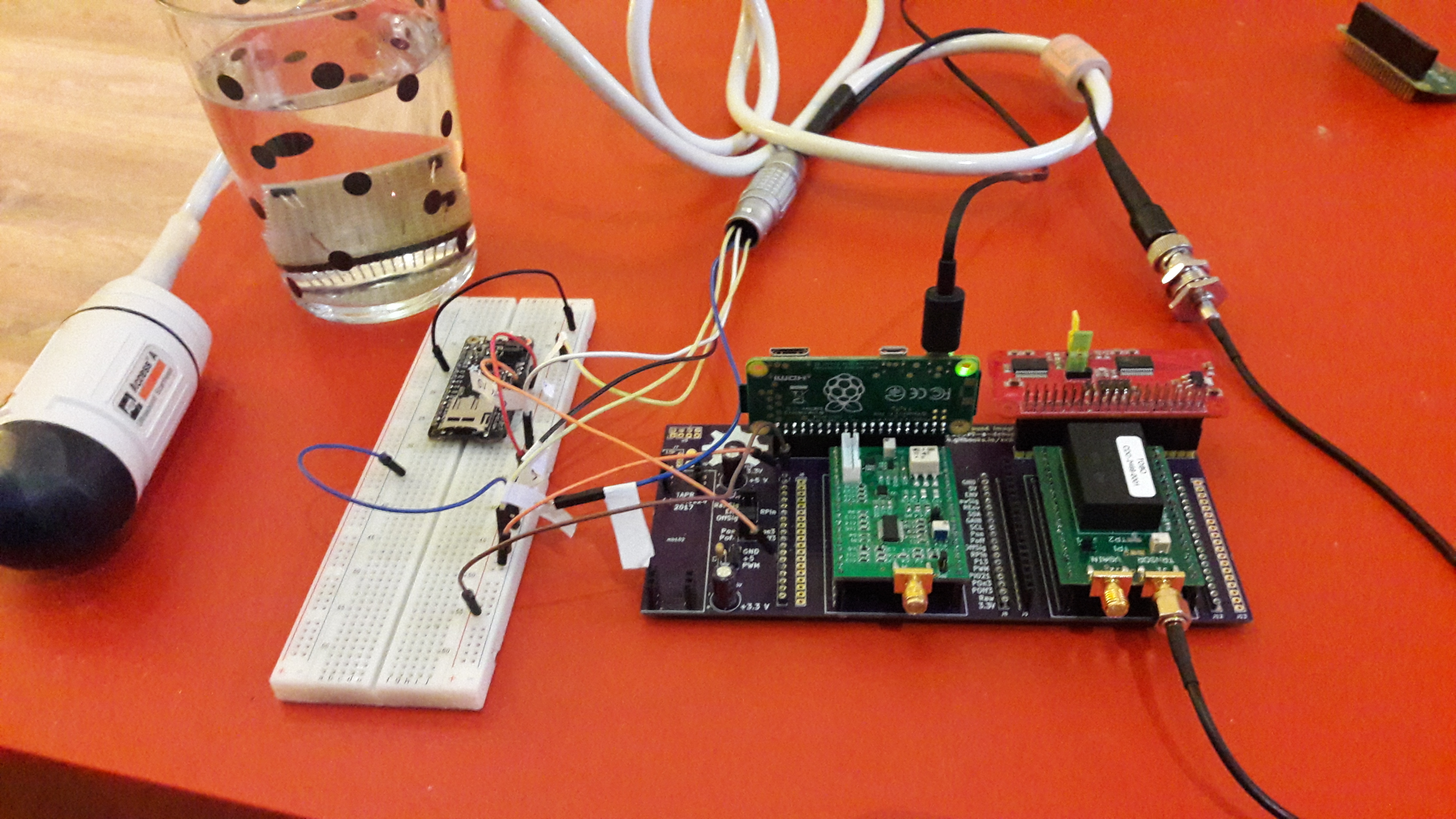
or as below:
TODO
- Lots
DONE
- Write the Quickstart
- Getting a board an soldering some ADCs
- Understand GPIO mem mapping
- Get raw data with offset vref/2
- Tests with a single ADC at 11Msps
- Produce a batch of rev2 elmo
People
- @ivan for his help on altium