Detailed notes of research
Notes on uC
Microcontrolers and chips
Microcontrolers
| ID | Name | Chip | Comments | ADC | Price | COmments |
|---|---|---|---|---|---|---|
| 1 | WiFiMCU | EMW3165 - STM32F411CE | Cortex-M4 core at 100MHz | 1_12-bit, 2.4 MSPS A/D converter: up to 16 channels | 8$ | Has wifi |
| 2 | Espruino Pico | STM32F401CDU6 | ARM Cortex M4, 384kb flash, 96kb RAM | 1_12-bit, 2.4 MSPS A/D converter | 24$ (Adafruit) | No wifi, smart USB plug, DSP instructions |
| 3 | Feather Wiced | STM32F205RG | 120MHz ARM Cortex M3 MCU + BCM43362 (avec un M3) | 3 x 12-bit, 0.5us ADCs with up to 24 channels and up to 6 MSPS in triple interleaved mode | 34$ | Has wifi, support for battery |
| 4 | STM32L471QE | STM32L471QE | NoP | 3_ 12-bit ADC 5 Msps, up to 16-bit with hardware oversampling | ?? | ?? |
| 5 | STM32L476 | STM32L476VGT6 | NOP | 3_ 12-bit ADC 5 Msps, up to 16-bit with hardware oversampling | 19$ dev-kit | Cheap, powerfull, nowifi |
| 6 | ESP32 | ?? | NoP | ?? | ?? | ?? |
| 7 | ESP8277 | Tensilica Xtensa LX106 | NoP | 80 MHz // 64 KiB of instruction RAM, 96 KiB of data RAM | 3$ | Has WiFi |
| 8 | Arduino Otto | STM32F469BIT6 | NoP | 3×12-bit, 2.4 MSPS ADC: up to 24 channels and 7.2 MSPS in triple interleaved mode | ?? | FAAAAT. Has Wifi through a ESP8266 |
| 9 | NanoPi m3 | Cortex-A53 S5P6818 SoC | ts dynamic frequency scales from 400M up to 1.4GHz. | ?? | ?? | Has WiFi |
| 10 | BBC Microbit | ?? | NoP | Not really a uC for us... | ?? | ?? |
| 11 | Nucleo F401RE | STM32F401RE | ?? | Joris working with this one | ?? | ?? |
| 12 | stm32f3 | ?? | NoP | 12-bit ADC 5 MSPS | 5-10$ | Analog and DSP with FPU ARM Cortex-M4 MCU with 64 Kbytes Flash, 72 MHz CPU, CCM, 12-bit ADC 5 MSPS |
| 13 | PIC32MZ | PIC32MZ | NoP | 12-bit, 28MSPS, 48-channel ADC module | 5$ | 200MHz/330 DMIPS, M-Class Core, DSP-enhanced core, 12-bit, 28MSPS, 48-channel ADC module |
- Feather (inclus un m3) : STM32F205 + BCM43362 qui a un m3
- Feather: meme chose que le photo, mais en compatible Arduino
- https://community.broadcom.com/servlet/JiveServlet/showImage/2-19579-3826/bcm43362-damosys.png
Studying chips
| ID | Name | Details | Comments |
|---|---|---|---|
| 1 | STM32F411CE | ||
| 2 | STM32F401CDU6 | ||
| 3 | stm32f407 | Recommended for data processing by Dmitry (GeekTimesRu) |
Other stuff
| ID | Name | Chip | Comments | ADC | Price | COmments |
|---|---|---|---|---|---|---|
| X | BBC MicroBit | A voir | NoP | ?? | ?? | ?? |
Notes on feather_WICED
Feather WICED
Facts
General
- Throughput test : https://learn.adafruit.com/introducing-the-adafruit-wiced-feather-wifi/throughput
- Built-in WiFi ( Broadcom radio )
- Built in battery adapter
- Double M3 ! Based on a STM32F205 -- 120MHz ARM Cortex M3 MCU + BCM43362 (Broadcom radio avec un M3)
- BSP required : https://learn.adafruit.com/introducing-the-adafruit-wiced-feather-wifi/get-the-wiced-bsp
Specs:
- STM32F205
Setup ?
Getting more on the ADC.
- https://forum.arduino.cc/index.php?topic=346761.0
- http://microcontroleurs.blogspot.fr/2015_07_01_archive.html?view=sidebar interessant!
- These two (fond on github) are lacking the 'ADC_PRE_PCLK2_DIV_2' was not declared in this scope
http://www.stm32duino.com/viewtopic.php?t=847 1Msps acquisition
RCC_ADCPRE_PCLK_DIV_2 can replace ADC_PRE_PCLK2_DIV_2 .. or so it seems
include
For getting more on the ADCs:
Notes on RPi0
RPi0 Oscilloscope
Ressources
Working ... with an external ADC. We need to test beforehands.
General
hacking camera CSI bus
Hat for SoC
SPI
- https://www.raspberrypi.org/documentation/hardware/raspberrypi/spi/README.md
- https://www.raspberrypi.org/forums/viewtopic.php?f=44&t=130616
- https://www.raspberrypi.org/forums/viewtopic.php?f=107&t=132494
- https://www.raspberrypi.org/forums/viewtopic.php?f=44&t=43442&p=347073
- http://richardhayler.blogspot.fr/2016/02/getting-started-with-esp8266-iot-phat.html
Resources pages
- http://bobdavis321.blogspot.fr/2013/06/arduino-powered-3-million-samples-per.html
- https://www.hackster.io/taifur/piscope-raspberry-pi-based-oscilloscope-01b6bb (modif kernel https://www.hackster.io/taifur/piscope-raspberry-pi-based-oscilloscope-01b6bb )
- Excellent resources : http://www.instructables.com/id/PiScope-Raspberry-Pi-based-Oscilloscope/
DIP ADC
- CA3306 -- 6 bits, up to 15Msps
- http://www.newark.com/analog-devices/ad7822bnz/analog-to-digital-converter-adc/dp/59K5579?aa=true&ost=adc&selectedCategoryId=&categoryId=800000004755&iscrfnonsku=false
- ANALOG DEVICES AD7822BNZ Analog to Digital Converter, 8 bit, 2 MSPS, 4.5 V, 5.5 V, DIP
Notes on ESP32
ESP32
- See the datasheet on (espressif site)[https://espressif.com/sites/default/files/documentation/esp_wroom_32_datasheet_en.pdf]
Details ?
ESP-WROOM-32 is a powerful, generic WiFi-BT-BLE MCU module that targets a wide variety of applications ranging from low power sensor networks to the most demanding tasks such as voice encoding, music streaming and MP3 decoding.
At the core of this module is the ESP32 chip, which is designed to be scalable and adaptive. There are 2 CPU cores that can be individually controlled or powered, and the clock frequency is adjustable from 80 MHz to 240 MHz. The user may also power off the CPU and make use of the low power coprocessor to constantly monitor the peripherals for changes or crossing of thresholds. ESP32 integrates a rich set of peripherals, ranging from capacitive touch sensors, Hall sensors, low noise sense amplifiers, SD card interface, Ethernet, high speed SDIO/SPI, UART, I2S and I2C.
The integration of Bluetooth, Bluetooth LE and Wi-Fi ensures that a wide range of applications can be targeted, and that it is future proof: using Wi-Fi allows a large physical range and direct connection to the internet through a Wi-Fi router, while using Bluetooth allows the user to conveniently connect to the phone or broadcast low energy beacons for its detection. The sleep current of the ESP32 chip is less than 5uA, making it suitable for battery powered and wearable electronics applications. ESP-WROOM-32 supports data rates up to 150 Mbps, and 22 dBm output power at the PA to ensure the widest physical range. As such the chip does offer industry leading specifications and the best optimized performance for electronic integration, range and power consumption, and connectivity.
ESP-WROOM-32 has Espressif’s long term support — ESP32 will be covered under Espressif’s longevity program and be available for the next 12 years. The design of ESP-WROOM-32 will be open-source when it has been fully optimized. Feedbacks about the module, chip, API or firmware can be sent to [email protected].
Notes on ESP8266
ESP8266
Factss
- throughput test : http://www.esp8266.com/viewtopic.php?f=5&t=245 + question posee sur http://www.esp8266.com/viewforum.php?f=6
- Livre: http://neilkolban.com/tech/esp8266/
- Question asked at http://stackoverflow.com/questions/37014547/esp8266-and-high-speed-external-adc
http://www.esp8266.com/wiki/doku.php?id=esp8266-module-family
- http://www.eevblog.com/forum/microcontrollers/esp8266-native-spi-hardware-driver/
- https://github.com/MetalPhreak/ESP8266_Microwire_EEPROM
- https://github.com/MetalPhreak/ESP8266_SPI_Driver
- Built-in low-power 32-bit CPU: can double as an application processor
- 802.11 b / g / n - Wi-Fi Direct (P2P), soft-AP
- http://www.instructables.com/id/ESP8266-ADC-Analog-Sensors/
- https://hackaday.io/project/4318-vu-meter-esp8266-ws2812b -- ESP8266+FFT+Teensy -- Person to contact!
https://forum.pjrc.com/threads/34095-Teensy-3-2-ESP8266-12Q-High-Speed-ADC-Websocket If you run the esp8266 wifi at 4.6 megabaud, you can get a minimum of 1 megabit per second throughput on wifi, a lot faster if your location does not have a ton of wifi signals, 2 mbit/s is typical. That is decent speed for my application.
ESP8266 -- ultra low power Micro 32bit CPU
- Excellent post - priority level : Important : http://www.eevblog.com/forum/microcontrollers/esp8266-native-spi-hardware-driver/
- SPI runs at 40Mhz. - so can be 2.4Msps 10bits
HSPI -> http://d.av.id.au/blog/esp8266-hardware-spi-hspi-general-info-and-pinout/
Les spores numériques sur snahck
Big brother : ESP32
Other versions
- Now, the ESP8266 v7 and v12, include an ADC (Analog digital converter) pin. This means that the ESP8266 module can process inputs from analog sensors. Light sensors, rheostats, force sensors, etc.
- Those with many GPIOs : ESP-04 et ESP-03
ESP-12-E/Q -- E-Series and ESP-14 have 22 pins available
Un dongle ESP8266 ! http://www.aliexpress.com/store/product/latest-ESP8266-Serial-WIFI-wireless-module-development-board-microcontroller-portable-USB-Dongle-in-case/939205_32576358152.html
- https://hackaday.io/project/9309-esp8266-dongle
- http://esp8266-re.foogod.com/wiki/Memory_Map
Some comments from Timothy
- Well, I have looked into that and figured out that the ESP8266 has 2 SPI interfaces (SPI and HSPI), the Flash memory uses the SPI interface, so we can attach the ADC to the HSPI interface and configure the SPI clock to between 1MHz to 80MHz depending on what we need. Therefore, it turns out it is possible to use an ADC with SPI interface, though it will involve some changes to the SPI registers but it can be done.
- The HSPI is definitely better than a software SPI. However, without the DMA (the HSPI isn't connected to it) the CPU will be distracted every time when a word is received via the HSPI. This means that the 2M words/sec stream will interrupt the 80 MHz CPU of the module on every 40-th cycle. Depending on the wifi software of the module, this may be a quite long delay for the system. Fortunatelly, we can try to speed up the module to 160 MHz in case of insufficient performance.
Some comments from Igor
- According to the PDF for ESP8266 it supports up to 40 MHz SPI clock (with default core clock) that is enough for our purpose. However, it doesn't have a DMA for the SPI master, so reading of the data from the ADC will be partially software based. This means that we can definitly pass the data through the SPI, but success of the further operations depends on the free CPU resources.
Fun piratebox
Notes on EMW3165
Fun about EMW3165
- EMW3165 : "All I see is an under 8USD STM32F411CE dev board with some wifi gadget"
- http://www.emw3165.com/
- http://hackaday.com/2015/07/13/new-part-day-the-esp8266-killer/
Notes on STM32F205_ref_manual
Notes on the STM32F205 Reference manual
Discussions are taking place to use the max speed on the Feather WICED:
ADC
- Configurable DMA data storage in Dual/Triple ADC mode
- Configurable delay between conversions in Dual/Triple interleaved mode
- ADC conversion time: 0.5 μs with APB2 at 60 MHz
- ADC supply requirements: 2.4 V to 3.6 V at full speed and down to 1.8 V at slower speed
- ADC input range: V REF– ≤ V IN ≤ V REF+
- DMA request generation during regular channel conversion
Fast conversion mode
It is possible to perform faster conversion by reducing the ADC resolution. The RES bits are used to select the number of bits available in the data register. The minimum conversion time for each resolution is then as follows:
- 12 bits: 3 + 12 = 15 ADCCLK cycles
- 10 bits: 3 + 10 = 13 ADCCLK cycles
- 8 bits: 3 + 8 = 11 ADCCLK cycles
- 6 bits: 3 + 6 = 9 ADCCLK cycles
Calibration
Using the feather WICED to produce a waveform:
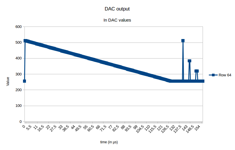
Versions of code so far
Compared to the waveform detailed above, gives the following acquisition:
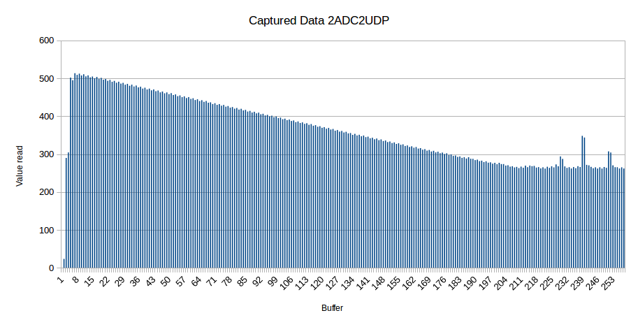
ADC common control register (ADC_CCR)
When the DMA mode is enabled (DMA bit set to 1 in the ADC_CR2 register), after each conversion of a regular channel, a DMA request is generated. This allows the transfer of the converted data from the ADC_DR register to the destination location selected by the software
- MULTI[4:0]: Multi ADC mode selection
- 10001 to 11001: Triple mode: ADC1, 2 and 3 working together
- 10111: interleaved mode only
Comment on the code
Initialization of the ADC
  // We configure the ADC1 and ADC2
  // Setting max sampling rate
  rcc_set_prescaler(RCC_PRESCALER_ADC, RCC_ADCPRE_PCLK_DIV_2);
  adc_set_sample_rate(ADC1, ADC_SMPR_1_5);
  adc_set_sample_rate(ADC2, ADC_SMPR_1_5);
  //  adc_set_sample_rate(ADC2, ADC_SMPR_3);

  //6=0110 for dual regular simultaneous mode
  // FOR STM32F1 -- DUALMOD[3:0]: Dual mode selection is on ADC control register 1 (ADC_CR1) - has to be changed
  // Bits 19:16 DUALMOD[3:0]: Dual mode selection
  // 7 is for interleaved mode.
  ADC1->regs->CR1 |= 7 << 16;

  //only one input in the sequence for both ADC: the channel 1

  adc_set_reg_seqlen(ADC1, 1);
  adc_set_reg_seqlen(ADC2, 1);
  adc_set_reg_seqlen(ADC3, 1);
  // Aiming at Interleaved mode on 1 channel in continuous conversion mode: triple ADC mode
  //channel 1 (PA1) on ADC1
  ADC1->regs->SQR1 |= 0;
  ADC1->regs->SQR2 = 0;
  ADC1->regs->SQR3 = 1; //00000.00000.00001
  //channel 1 (PA1) on ADC2
  ADC2->regs->SQR1 |= 0;
  ADC2->regs->SQR2 = 0; //00000.00000.00000
  ADC2->regs->SQR3 = 1; //00000.00000.00010
  //channel 1 (PA1) on ADC3
  ADC3->regs->SQR1 |= 0;
  ADC3->regs->SQR2 = 0; //00000.00000.00000
  ADC3->regs->SQR3 = 1; //00000.00000.00010
Acquisition
Acquisition takes place in a loop, where 2*BUFFERSIZE data is acquired. Values from ADC1 and ADC2 go into val1 and val2.
    while (i < BUFFERSIZE) {
      // ADC : page 212 to 254 in the reference manual

      //start conversion
      ADC1->regs->CR2 |= ADC_CR2_SWSTART;
      ADC2->regs->CR2 |= ADC_CR2_SWSTART;

      // Wait the end of the conversion
      while (!(ADC1->regs->SR & ADC_SR_EOC)) ;
      while (!(ADC2->regs->SR & ADC_SR_EOC)) ;

      // Get the values converted from the two ADCs.
      // They are sharing the same channel, in interleaved mode
      val1[i] = (int16)(ADC1->regs->DR & ADC_DR_DATA);
      val2[i] = (int16)(ADC2->regs->DR & ADC_DR_DATA);
      i++;
   }
Notes on R2R_DAC
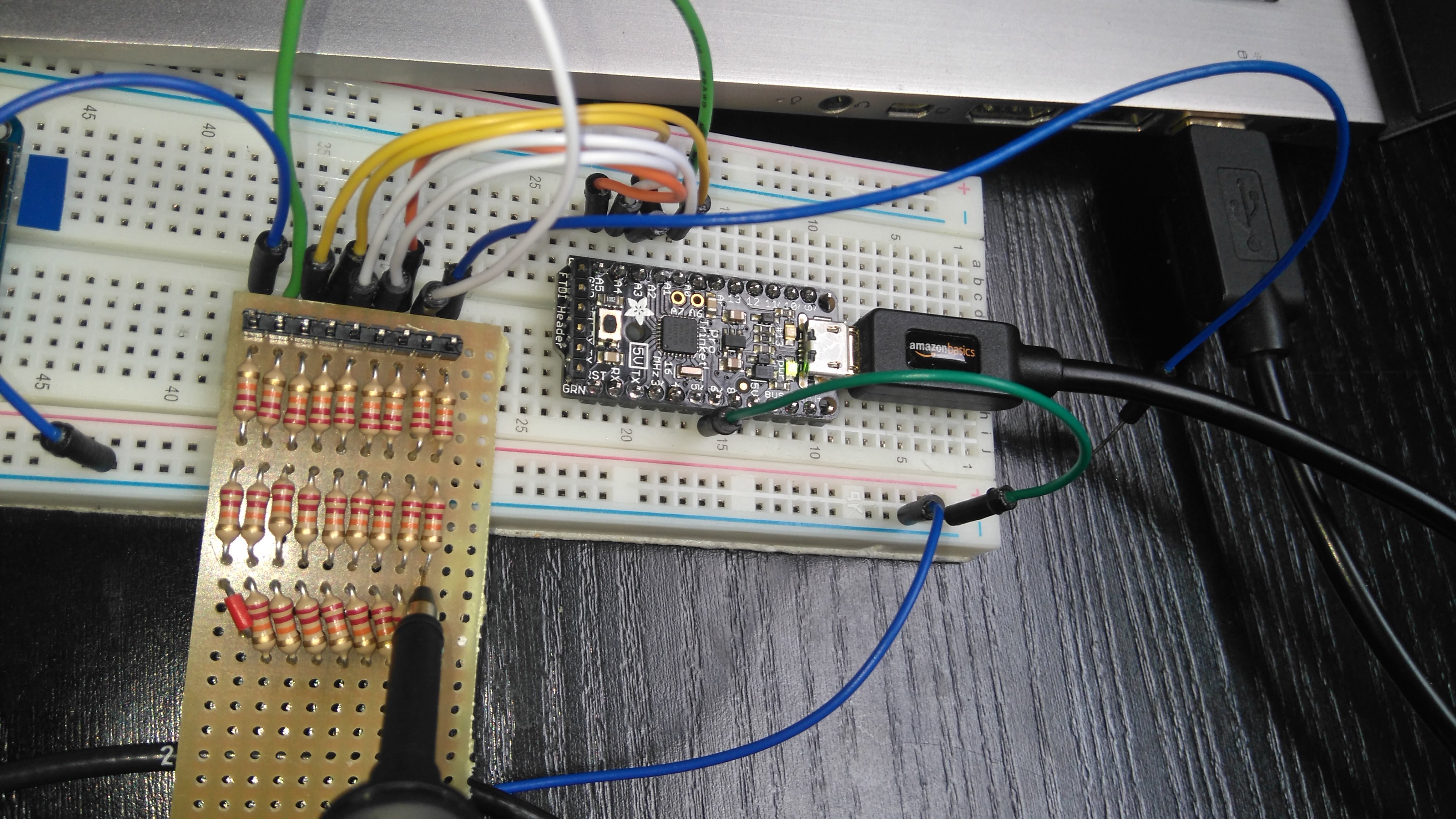
Playing with a R2R resistor ladder, AKA the quick DAC.
Playing with a 22kO R ladder
An R–2R Ladder is a simple and inexpensive way to perform digital-to-analog conversion, using repetitive arrangements of precise resistor networks in a ladder-like configuration. A string resistor ladder implements the non-repetitive reference network.

Let's try to see if we can do some signal with it!
Playing with it
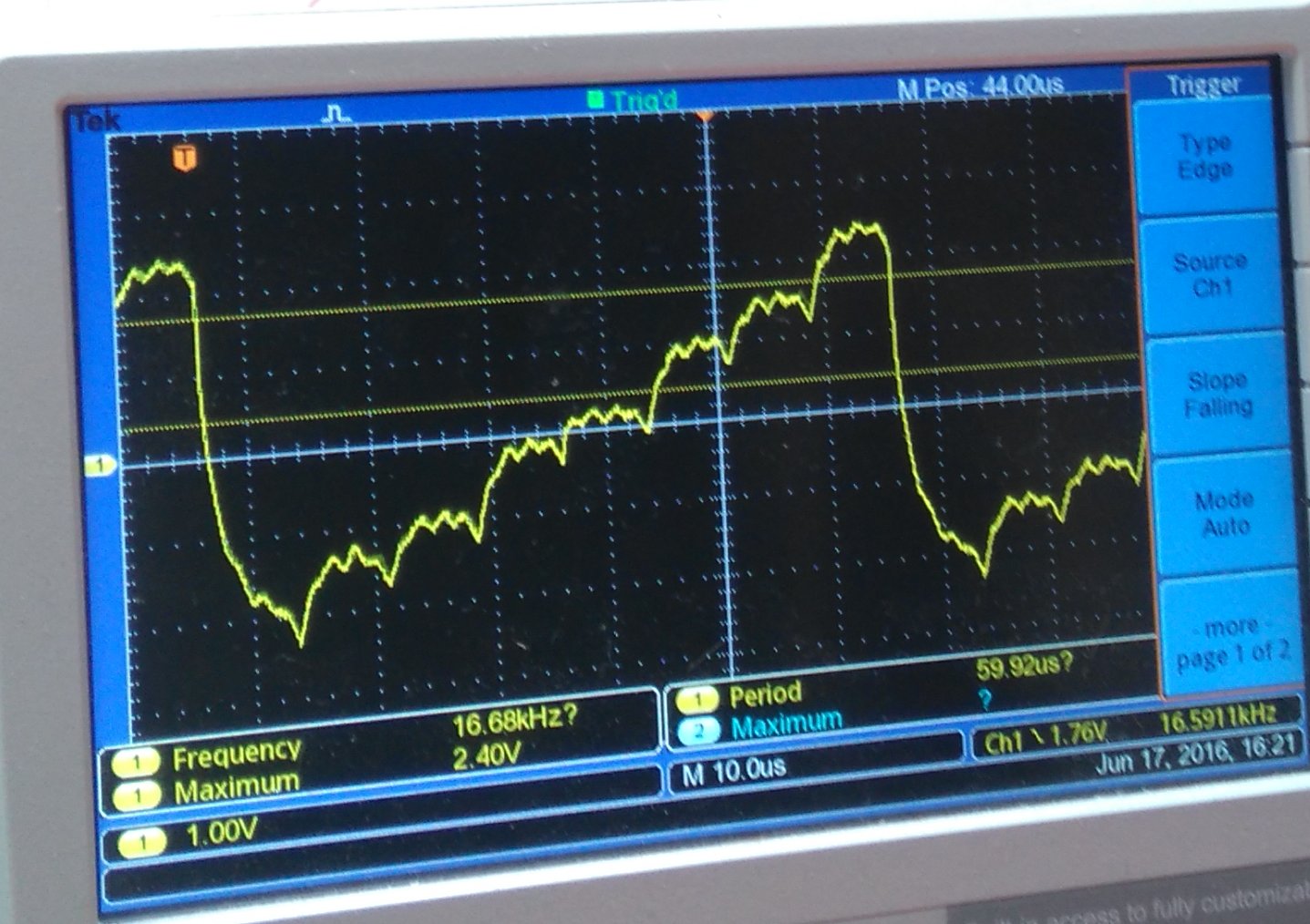
What does it look like?
Playing with the variant 2 of the code below (increase, bit by bit, over 6 bits)
Limitations
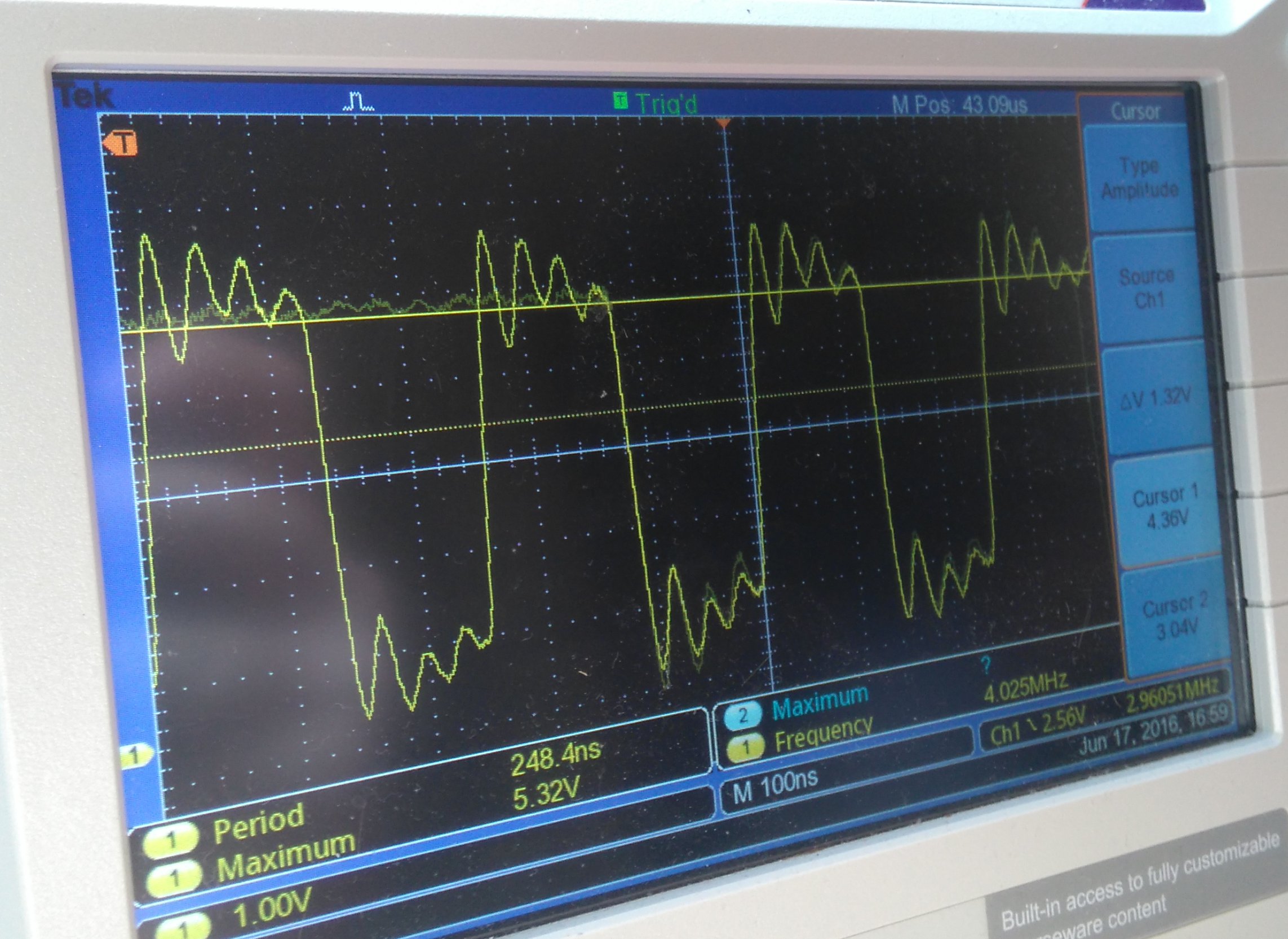
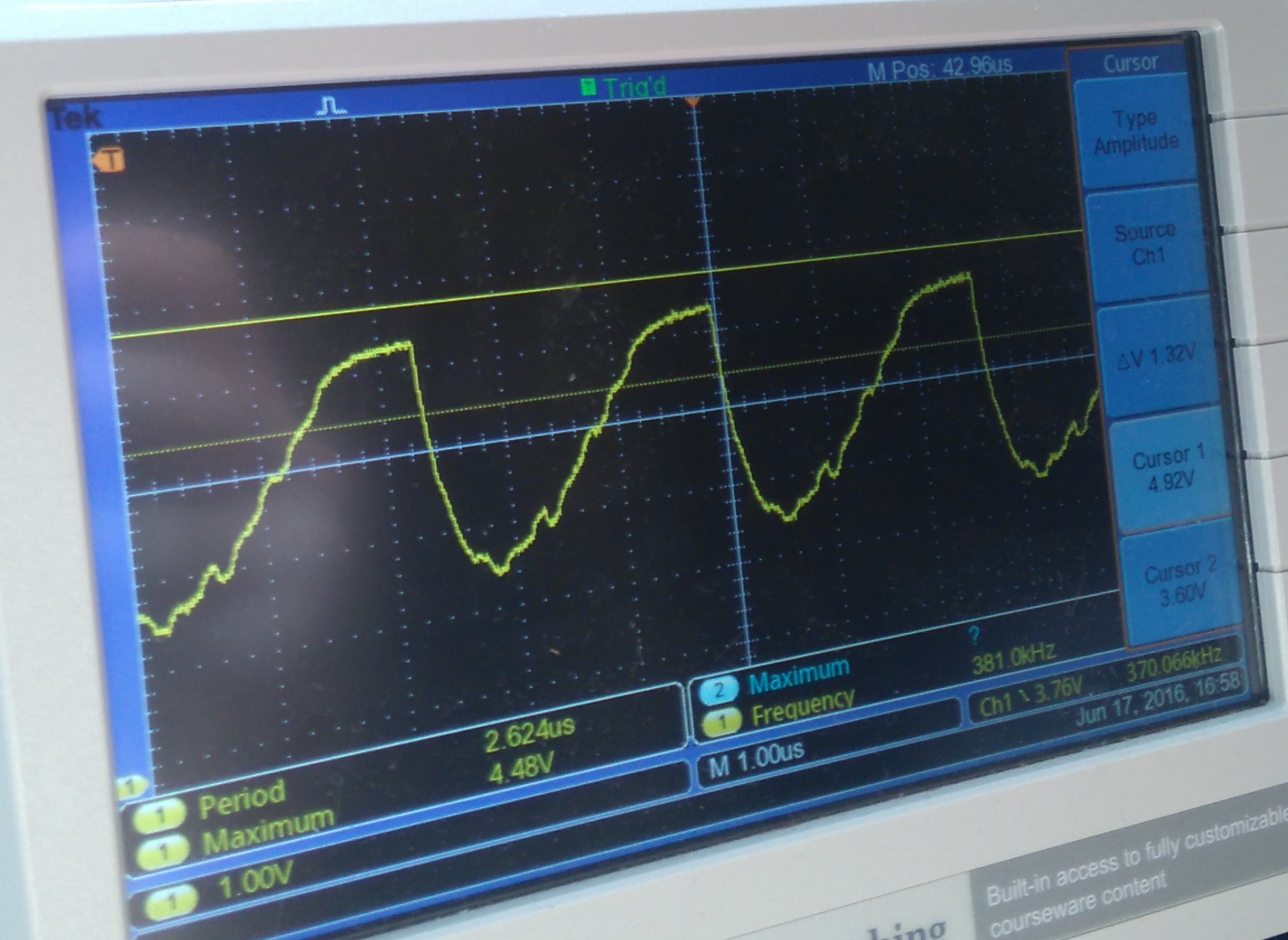
With the variant 2, the quickest signal is at ~5MHz
But when feeding the ladder, it slows... see characteristic time below
Conclusions
Let's try something with the variant 1, feeding the Arduino a translation of one image! It has 28K of flash, let' remove 2k for code, 26kb, using 6-bit accuracy, is 64, leaves 4k points.
Trinket pro codes
Variant 1
The quickest so far
void setup()
 {
  DDRC = 255; // set PORTD (Pins 0-7) to outputs
  PORTC = 0;  // Set all pins LOW
 }

void loop() {
   PORTC = B0000000;
   PORTC = B0000001;
   PORTC = B0000010;
   PORTC = B0000011;
   PORTC = B0000100;
   PORTC = B0000101;
   PORTC = B0000110;
   PORTC = B0000111;
   PORTC = B0001000;
   PORTC = B0001001;
   PORTC = B0001010;
   PORTC = B0001011;
   PORTC = B0001100;
   PORTC = B0001101;
   PORTC = B0001110;
   PORTC = B0001111;
}
Variant 2
Using autoincrement of PORTC:
void setup()
{
  DDRC = 255; // set PORTD (Pins 0-7) to outputs
  PORTC = 0;  // Set all pins LOW
}

void loop() {
   PORTC++;
}
